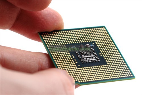
Ultra-Small Size PCB Manufacturer
Ultra-Small Size PCB Manufacturer,Ultra-small size PCBs are designed to meet the demands of highly compact electronic devices where space is at a premium. These PCBs feature a minimized footprint while incorporating intricate circuit designs and advanced technologies. The manufacturing process involves precision engineering and advanced materials to ensure reliable performance despite the reduced size. Ultra-small PCBs are commonly used in applications such as wearable technology, IoT devices, and miniature sensors. Their ability to fit into tight spaces while delivering robust electrical performance and functionality makes them essential for modern electronics that require both compactness and efficiency.
What is Ultra-Small Size PCB?
Ultra-Small Size PCBs are printed circuit boards designed to fit in exceptionally compact spaces, often used in applications where space is at a premium. These PCBs are characterized by their minimized dimensions, enabling integration into small devices such as wearable electronics, medical implants, and compact consumer gadgets.
The design and manufacturing of ultra-small PCBs present several challenges. Engineers must carefully consider component placement, trace routing, and soldering techniques to ensure reliability and functionality within the constrained space. Advanced technologies like microvias, fine-pitch components, and multi-layer construction are often employed to achieve the required miniaturization while maintaining performance standards.
Materials used in ultra-small PCBs are typically high-performance to withstand the mechanical and thermal stresses encountered in small, densely packed devices. These materials often include advanced laminates with high thermal conductivity and low dielectric loss to support high-speed signal integrity and thermal management.
Additionally, the manufacturing process for ultra-small PCBs involves precise photolithography and etching techniques to produce fine-featured circuits. Surface mount technology (SMT) is commonly used for component assembly, allowing for the placement of tiny components on the PCB surface with high density.
Overall, ultra-small size PCBs play a crucial role in the advancement of compact and portable electronics, driving innovation in various fields by enabling the integration of sophisticated technology into smaller and more versatile devices.

Ultra-Small Size PCB Manufacturer
What is the Ultra-Small Size PCB Design Guidelines?
Designing ultra-small size PCBs requires meticulous attention to detail to ensure functionality and reliability in constrained spaces. Here are some key guidelines for designing ultra-small size PCBs:
- Component Selection: Opt for miniature components with fine-pitch packages to maximize space utilization. Use components that are compatible with surface-mount technology (SMT) for efficient placement and assembly.
- Layout Optimization: Prioritize efficient layout by minimizing trace lengths and avoiding unnecessary routing. Use a compact footprint for components and consider stackable designs to conserve space.
- High-Density Interconnects: Employ advanced technologies like microvias and fine-pitch traces to fit more functionality into a smaller area. Multi-layer PCBs can be beneficial for managing complex circuitry within limited space.
- Thermal Management: Incorporate thermal vias and heat sinks to dissipate heat effectively. Use materials with high thermal conductivity to ensure that the PCB can handle the thermal stresses associated with high-density designs.
- Signal Integrity: Maintain signal integrity by carefully routing high-speed signals and minimizing interference. Implement proper grounding and shielding techniques to reduce noise and ensure reliable performance.
- Manufacturing Constraints: Be aware of manufacturing limitations such as minimum trace width and spacing, and ensure that your design adheres to these constraints. Use design-for-manufacturing (DFM) practices to avoid potential issues during production.
- Mechanical Considerations: Account for mechanical stress and ensure that the PCB design accommodates any potential flexing or impact. Use appropriate materials and design features to enhance durability and resilience.
- Testing and Debugging: Design with test points and debugging features in mind to facilitate troubleshooting and quality control. Consider built-in diagnostics and ensure accessibility for maintenance.
By following these guidelines, designers can effectively create ultra-small PCBs that meet performance requirements while fitting into the compact form factors of modern electronic devices.
The advantages of Ultra-Small Size PCB
Ultra-small size PCBs offer several advantages that make them ideal for use in compact and portable electronic devices. Here are the key benefits:
- Space Efficiency:Ultra-small PCBs maximize the use of limited space within electronic devices. This allows for more compact and lightweight designs, which is crucial for portable gadgets like wearables and handheld devices.
- Enhanced Portability: By reducing the size of the PCB, manufacturers can design more portable and convenient products. This is especially important in industries such as consumer electronics, medical devices, and automotive applications, where space and weight are critical factors.
- Increased Design Flexibility: Smaller PCBs allow for more innovative and flexible product designs. Designers can incorporate advanced features and functionality into smaller form factors, leading to more sophisticated and versatile devices.
- Cost Efficiency: In some cases, ultra-small PCBs can lead to cost savings by reducing the amount of raw materials used and potentially lowering manufacturing and assembly costs. This is particularly true when high-density interconnects and efficient layouts minimize material waste.
- Improved Performance: Advances in materials and manufacturing techniques for ultra-small PCBs can enhance overall performance. For example, high-performance laminates and precise routing can improve signal integrity and thermal management.
- Competitive Advantage: Devices that incorporate ultra-small PCBs often offer a competitive edge by providing more compact, feature-rich solutions compared to traditional designs. This can be a significant factor in markets where miniaturization is a key selling point.
- Integration of Advanced Technologies: Ultra-small PCBs can accommodate advanced technologies such as IoT sensors and wireless communication modules, enabling the development of sophisticated, miniaturized electronic systems with cutting-edge capabilities.
By leveraging these advantages, manufacturers can develop innovative products that meet the growing demand for smaller, more efficient, and versatile electronic devices.
What is the Ultra-Small Size PCB Fabrication Process?
The fabrication process for ultra-small size PCBs involves several precise and specialized steps to ensure high quality and performance within compact dimensions. Here’s an overview of the key stages in the fabrication process:
- Design and Layout: The process begins with creating a detailed PCB design using advanced CAD software. Designers focus on optimizing component placement, trace routing, and ensuring compliance with design rules specific to ultra-small PCBs, such as fine-pitch components and microvias.
- Material Selection: Choose appropriate high-performance materials that can handle the specific requirements of ultra-small PCBs. This often includes advanced laminates with low dielectric loss and high thermal conductivity to support high-speed signal transmission and thermal management.
- Photolithography: A photolithographic process is used to transfer the PCB design onto the substrate. This involves coating the substrate with a photosensitive material, exposing it to light through a mask with the PCB design, and then developing the image to define the copper patterns.
- Etching: The exposed copper areas are etched away to leave behind the desired circuit patterns. For ultra-small PCBs, precision etching is crucial to create fine traces and pads without damaging the delicate features.
- Drilling: Microvias and other small holes are drilled into the PCB to facilitate connections between different layers and components. This step requires high-precision drilling equipment to accommodate the tiny features of ultra-small PCBs.
- Plating and Deposition: After drilling, the PCB undergoes electroplating to deposit a thin layer of metal (usually copper) inside the holes and on the surface to establish electrical connections. Additional layers, such as solder mask and silkscreen, are also applied as needed.
- Solder Mask Application: A solder mask is applied to protect the circuit traces and prevent solder bridges during assembly. For ultra-small PCBs, precise application is necessary to avoid covering fine-pitch components and traces.
- Surface Finish: A surface finish, such as ENIG (Electroless Nickel Immersion Gold) or OSP (Organic Solderability Preservative), is applied to enhance solderability and protect the PCB’s exposed copper surfaces.
- Inspection and Testing: The fabricated PCB undergoes rigorous inspection and testing to ensure it meets design specifications and quality standards. This includes visual inspection, electrical testing, and functionality verification.
- Cutting and Packaging: Finally, the PCB is cut from the panel, and any additional processing, such as edge radiusing or hole plating, is completed. The PCBs are then packaged for shipment or further assembly.
These steps ensure that ultra-small PCBs are manufactured with high precision and reliability, suitable for integration into compact and sophisticated electronic devices.
The application of ceramic Ultra-Small Size PCB
Ceramic ultra-small size PCBs are increasingly used in various advanced applications due to their superior properties. Here are the key applications of ceramic ultra-small size PCBs:
- Medical Devices: In medical technology, ceramic ultra-small PCBs are used in implantable devices, such as pacemakers and hearing aids. Their biocompatibility, high thermal conductivity, and reliability make them ideal for these sensitive applications.
- Wearable Electronics: Ceramic ultra-small PCBs are crucial for wearable devices like smartwatches and fitness trackers. Their compact size and durability support the integration of advanced sensors and communication modules in a small form factor.
- Aerospace and Defense: In aerospace and defense applications, ceramic ultra-small PCBs are used in critical systems such as navigation and communication equipment. Their high temperature resistance and stability under harsh conditions are essential for these high-reliability applications.
- High-Frequency and RF Applications: Ceramic PCBs are preferred in high-frequency and RF (radio frequency) applications due to their low dielectric loss and stable electrical performance. They are used in RF communication systems, antennas, and radar systems where signal integrity is crucial.
- Automotive Electronics: In the automotive industry, ceramic ultra-small PCBs are utilized in advanced driver assistance systems (ADAS), engine control units (ECUs), and other critical electronic systems. Their ability to withstand high temperatures and vibrations makes them suitable for automotive environments.
- Telecommunications:Ceramic ultra-small PCBs are employed in telecommunications equipment such as base stations and network routers. Their excellent thermal management and electrical performance help ensure reliable operation in high-demand scenarios.
- Consumer Electronics: In consumer electronics, ceramic ultra-small PCBs are used in compact devices like smartphones and tablets. Their small size and high performance support the integration of complex circuits and functionalities into portable devices.
- Industrial Automation: For industrial automation and control systems, ceramic ultra-small PCBs offer robust performance and durability. They are used in sensors, controllers, and communication modules that require high reliability in demanding environments.
By leveraging the advantages of ceramic materials, such as high thermal conductivity, low dielectric loss, and mechanical robustness, ceramic ultra-small size PCBs enable the development of advanced, reliable, and compact electronic systems across various high-tech and demanding applications.
FAQs about Ultra-Small Size PCB
What is an ultra-small size PCB?
An ultra-small size PCB is a printed circuit board designed with minimized dimensions to fit into compact spaces within electronic devices. It is used in applications where space is limited and compact form factors are essential.
What are the key benefits of ultra-small size PCBs?
Key benefits include space efficiency, enhanced portability, increased design flexibility, improved performance, cost efficiency, and a competitive advantage by enabling innovative, compact device designs.
What challenges are associated with designing ultra-small size PCBs?
Challenges include managing component placement, ensuring reliable trace routing, maintaining signal integrity, and addressing thermal management within constrained dimensions. Precision in manufacturing and assembly is also critical.
What materials are used for ultra-small size PCBs?
Common materials include high-performance laminates with low dielectric loss and high thermal conductivity. These materials support high-speed signal transmission and effective thermal management.
What fabrication techniques are used for ultra-small size PCBs?
Fabrication techniques include precise photolithography, fine-pitch etching, microvia drilling, electroplating, and advanced surface finishes. These techniques ensure high precision and functionality in small PCB designs.
Where are ultra-small size PCBs commonly used?
They are commonly used in medical devices, wearable electronics, aerospace and defense applications, high-frequency RF systems, automotive electronics, telecommunications, consumer electronics, and industrial automation.


