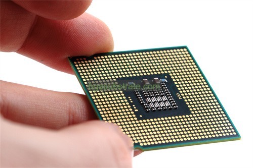
TU-933+ Substrate Изготовитель
ТУ-933+ Производитель подложек,TU-933+ substrate is an innovative laminate designed for high-performance applications in the RF and microwave sectors. Он отличается низкой диэлектрической проницаемостью и малыми тангенсом потерь, ensuring exceptional signal integrity and minimal signal degradation. The substrate is engineered for high thermal stability and low moisture absorption, making it reliable in demanding environments. Its compatibility with fine-line processing supports intricate multilayer designs and high-density interconnects. TU-933+ is particularly suited for use in telecommunications, аэрокосмический, and advanced automotive applications, where its robust performance characteristics help meet the stringent requirements of modern electronic systems.
What is TU-933+ Substrate?
The TU-933+ substrate is a high-performance circuit board material specifically designed for high-frequency and high-temperature applications. Its main features include excellent electrical insulation and low-loss characteristics, making it highly suitable for RF (radio frequency) и микроволновые цепи. The dielectric constant of TU-933+ typically ranges from 3.0 Кому 3.2, with a low temperature coefficient, allowing it to maintain good electrical performance over a wide temperature range.
Дополнительно, TU-933+ has high thermal conductivity, which enables effective heat dissipation, reducing performance degradation due to rising temperatures. В процессе производства, advanced techniques are employed to ensure uniform thickness and surface flatness, further enhancing the PCB’s machinability and signal integrity.
TU-933+ substrates are commonly used in mobile phones, Спутниковая связь, Радиолокационные системы, and other high-frequency electronic devices. Due to their superior electrical and mechanical properties, TU-933+ has become an increasingly popular material choice in high-end electronic products. Suitable for multilayer circuit board manufacturing, TU-933+ provides designers with greater flexibility and performance assurance.
Резюме, the TU-933+ substrate excels in high-frequency and high-temperature environments, making it an indispensable foundational material in cutting-edge electronic products.

ТУ-933+ Производитель подложек
What is the TU-933+ Substrate Design Guidelines?
Рекомендации по проектированию TU-933+ substrate Обычно включают в себя следующие ключевые соображения:
- Наложение слоев: Ensure proper layer configuration for signal, ground, and power layers to minimize impedance discontinuities.
- Ширина и интервал между трассами: Calculate trace widths based on current-carrying capacity and desired impedance. Maintain appropriate spacing between traces to prevent crosstalk.
- Проектирование переходных отверстий: Use appropriate via sizes and types (например., слепой, buried, or through vias) to ensure reliable electrical connections. Keep via placements optimized for signal integrity.
- Управление температурным режимом: Consider thermal vias and copper pours to enhance heat dissipation, особенно в системах с высокой мощностью.
- Ground Plane: Utilize a solid ground plane to reduce electromagnetic interference (EMI) and enhance overall signal integrity.
- Управление импедансом: Design transmission lines with controlled impedance, taking into account the substrate’s dielectric properties and the desired characteristic impedance.
- Design for Manufacturability (ГФ.): Follow guidelines for minimum trace widths, интервал, and hole sizes based on the manufacturer’s capabilities to ensure successful fabrication.
- Simulation and Testing: Utilize simulation tools for signal integrity and thermal analysis during the design phase. Plan for testing to validate performance after fabrication.
- Механические соображения: Ensure that the substrate is compatible with assembly processes (например., soldering, bonding) and that mechanical stresses are accounted for in the design.
By adhering to these guidelines, designers can optimize the performance and reliability of circuits utilizing TU-933+ substrates in high-frequency applications.
The advantages of TU-933+ Substrate
TU-933+ is a type of high-performance PCB substrate known for its exceptional properties. Here are some advantages of using TU-933+:
- Высокая теплопроводность: TU-933+ offers superior heat dissipation, making it ideal for applications that generate significant heat. This property helps in maintaining the reliability and longevity of electronic components.
- Excellent Electrical Properties:The substrate has low dielectric loss and high dielectric constant, which contributes to better signal integrity and reduced signal attenuation. This is crucial for high-frequency applications.
- Stable Mechanical Properties: TU-933+ provides good mechanical stability, which helps in maintaining the integrity of the PCB under various conditions, including temperature fluctuations and mechanical stress.
- Thermal Expansion Matching: The thermal expansion coefficient of TU-933+ is closely matched with that of copper, reducing the risk of delamination and other reliability issues during thermal cycling.
- High Frequency Performance: Its electrical properties make it suitable for high-frequency applications, such as RF and microwave circuits, where maintaining signal quality is essential.
- Good Processability: TU-933+ is known for its ease of processing, which can lead to lower manufacturing costs and higher yield rates in PCB production.
- Совместимость с бессвинцовой пайкой: The substrate performs well with lead-free soldering processes, which is important for meeting modern environmental and regulatory standards.
These advantages make TU-933+ a preferred choice for demanding electronic applications where performance, надёжность, and durability are critical.
What is the TU-933+ Substrate Fabrication Process?
The fabrication process for TU-933+ substrates typically involves several key steps to ensure high-quality performance and reliability. Here’s a general overview:
- Подготовка материала: The TU-933+ substrate material, which consists of a specific blend of ceramic and resin, is prepared and cut to the desired size and shape. This step involves ensuring that the raw material meets the required specifications for thermal and electrical properties.
- Cleaning: The substrate material is thoroughly cleaned to remove any contaminants that could affect adhesion and overall performance. This often involves ultrasonic cleaning and rinsing.
- Coating: A thin layer of adhesive or bonding material is applied to the substrate. This layer is crucial for ensuring proper adhesion of the copper foil and other layers.
- Copper Foil Lamination: Copper foil is laminated onto the substrate using heat and pressure. The copper foil acts as the conductive layer for the PCB. The lamination process ensures a strong bond between the copper and the substrate.
- Drilling and Imaging: Holes and vias are drilled into the substrate as needed. Then, imaging is performed to create the desired circuit patterns on the copper layer. This usually involves applying a photosensitive resist layer, воздействие на него ультрафиолетового излучения через маску, and developing the pattern.
- Офорт: The exposed copper is etched away to form the circuit patterns. This step involves using chemicals to remove the unwanted copper, leaving behind the desired circuitry.
- Металлизация: In cases where additional thickness is required or for via plating, a plating process is used to deposit a layer of metal into the holes or vias.
- Final Inspection and Testing: The finished substrates undergo rigorous inspection and testing to ensure they meet the required electrical and mechanical specifications. This may include visual inspections, Электрические испытания, and thermal cycling tests.
- Резка и отделка: The substrates are cut to their final dimensions and any additional finishing processes are applied, such as edge routing or surface treatments.
- Упаковка: The completed substrates are carefully packaged to prevent damage during shipping and handling.
Each of these steps is carefully controlled to ensure that the TU-933+ substrates meet the high standards required for high-frequency and high-performance applications.
The application of ceramic TU-933+ Substrate
Ceramic TU-933+ substrates are used in various high-performance and demanding electronic applications due to their superior thermal and electrical properties. Вот некоторые ключевые области применения:
- High-Frequency RF and Microwave Circuits: TU-933+ substrates are ideal for RF (Радиочастота) and microwave applications due to their low dielectric loss and high thermal conductivity, which help in maintaining signal integrity and reducing heat buildup.
- Power Amplifiers: In power amplifier circuits, particularly those used in telecommunications and broadcasting, TU-933+ provides the thermal management and electrical performance needed for efficient operation and reliability.
- Аэрокосмическая и оборонная промышленность: These substrates are used in aerospace and defense applications where high reliability and performance are critical. Their stability under extreme conditions and ability to handle high frequencies make them suitable for satellite communications and radar systems.
- Медицинские приборы: For medical electronics, TU-933+ substrates offer the high performance needed for precision instruments and devices that require stable operation in challenging environments.
- Автомобильная электроника: В автомобильной промышленности, TU-933+ is used for high-frequency components and power electronics, such as those found in advanced driver-assistance systems (АДАС) and infotainment systems.
- Электросвязь: The substrate’s performance characteristics are advantageous for telecommunications equipment, including base stations and network infrastructure, where high signal quality and thermal management are essential.
- High-Performance Computing: TU-933+ is used in computing applications where high-frequency signal integrity and efficient heat dissipation are required, such as in high-speed data processors and servers.
- Military Communication Systems: The substrate’s durability and performance make it suitable for use in military communication systems, where reliability and resistance to environmental stresses are crucial.
Полный, TU-933+ substrates are chosen for their ability to maintain performance in high-frequency and high-power applications, as well as their ability to manage thermal challenges effectively.
FAQs about TU-933+ Substrate
What is TU-933+?
TU-933+ is a high-performance ceramic PCB substrate known for its excellent thermal conductivity, Низкие диэлектрические потери, and high-frequency performance. It is used in applications requiring high signal integrity and efficient heat dissipation.
What are the main advantages of TU-933+?
TU-933+ offers high thermal conductivity, excellent electrical properties (low dielectric loss and high dielectric constant), stable mechanical properties, and good processability. It is also compatible with lead-free soldering.
In which applications is TU-933+ typically used?
TU-933+ is commonly used in RF and microwave circuits, power amplifiers, aerospace and defense systems, Медицинские приборы, Автомобильная электроника, электросвязь, high-performance computing, and military communication systems.
What is the fabrication process for TU-933+ substrates?
The fabrication process involves material preparation, cleaning, coating with adhesive, copper foil lamination, drilling and imaging, офорт, металлизация, inspection and testing, cutting and finishing, and packaging.
How does TU-933+ compare to other substrates in terms of thermal management?
TU-933+ provides superior thermal management compared to many other substrates due to its high thermal conductivity. This helps in effectively dissipating heat and maintaining the reliability of electronic components.
What are the electrical properties of TU-933+?
TU-933+ features low dielectric loss and a high dielectric constant, which contribute to minimal signal attenuation and excellent signal integrity, Что делает его пригодным для высокочастотных применений.
Is TU-933+ compatible with lead-free soldering processes?
Да, TU-933+ substrates are compatible with lead-free soldering processes, which is important for meeting environmental and regulatory standards.
 Название вашего сайта


