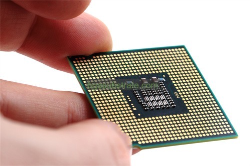
Flip Chip Substrate Изготовитель
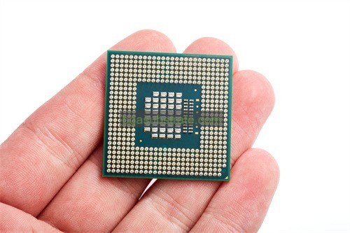
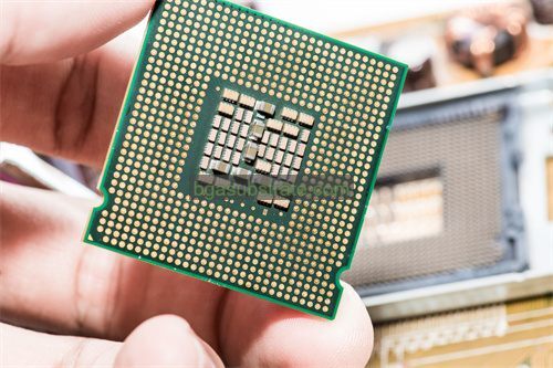
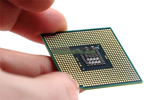
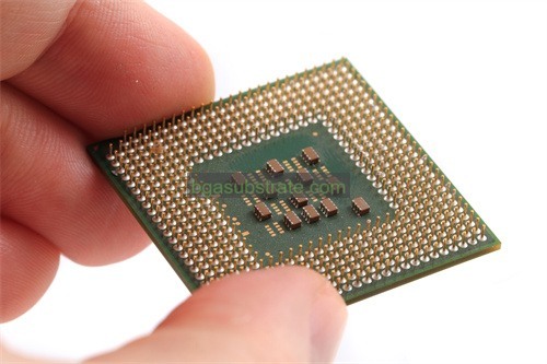
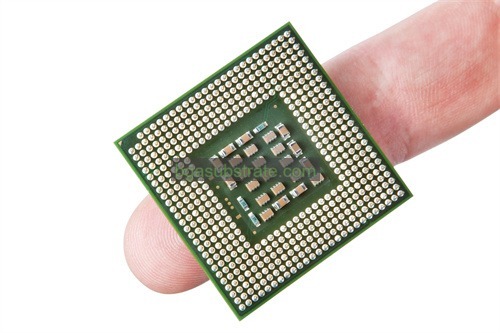
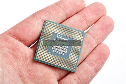
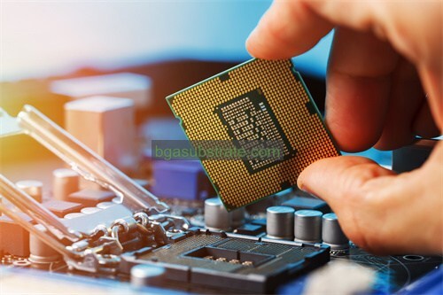
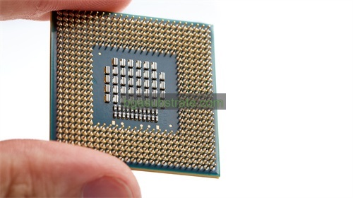
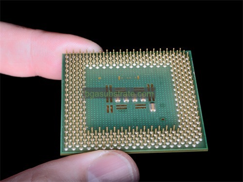
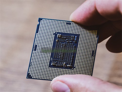
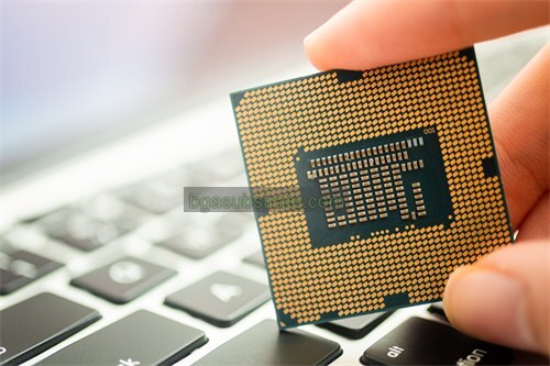
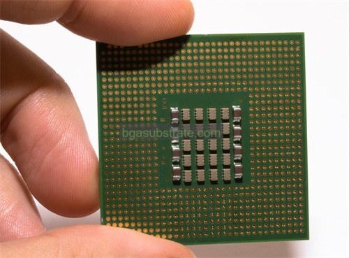
Производитель подложек для флип-чипов,Flip chip substrates are specialized platforms used in the packaging of semiconductor devices where the chip is flipped upside down and connected directly to the substrate using solder bumps. This technique allows for shorter electrical paths, reducing signal loss and improving performance, especially in high-frequency applications. Flip chip substrates provide excellent thermal dissipation and mechanical support, making them ideal for high-power and high-density applications. They are commonly used in processors, graphics cards, and other advanced electronics that require robust and reliable connections. The use of flip chip substrates enables compact designs and efficient integration of multiple functions within a single package.
Что такое Flip Chip Substrate?
A Flip Chip Substrate is a crucial component in advanced electronic packaging, used to mount integrated circuits (ИС) onto a printed circuit board (PCB) or another substrate. Unlike traditional packaging methods where the IC is mounted on top of the substrate, flip chip technology involves flipping the IC upside down and bonding it directly to the substrate using solder bumps or conductive pads.
In this packaging method, the IC’s active side, containing the circuitry, is attached to the substrate, while the non-active side is exposed. This direct connection significantly reduces the signal path length between the IC and the substrate, which enhances performance by minimizing signal delay and increasing electrical efficiency. The solder bumps or pads, also known as flip chip bumps, provide electrical and mechanical connections, allowing for high-density interconnections and better thermal management.
Flip chip substrates are often made from materials with high thermal conductivity and low electrical resistance, such as high-performance FR4, ceramics, or advanced composite materials. The choice of substrate material impacts the thermal dissipation and overall reliability of the chip. Дополнительно, flip chip technology supports finer pitch connections and higher pin counts, making it suitable for applications in high-performance computing, электросвязь, и бытовая электроника.
This technology not only improves electrical performance and reliability but also enables more compact and lightweight designs, crucial for modern electronic devices. The ability to directly bond the IC to the substrate allows for more efficient heat dissipation and reduces the package size, leading to advancements in device miniaturization and functionality.

Производитель подложек для флип-чипов
Что такое Flip Chip Substrate Рекомендации по проектированию?
Flip Chip Substrate Design Guidelines are essential for ensuring the performance, надёжность, and manufacturability of flip chip packages. These guidelines focus on various aspects of substrate design to optimize electrical and thermal performance while minimizing manufacturing issues. Here are some key guidelines:
- Die Size and Pad Layout: The design should accommodate the size of the semiconductor die and the arrangement of the solder bumps. The layout of the pads on the substrate must align precisely with the bumps on the die to ensure reliable connections.
- Solder Bump Configuration: The size, pitch, and placement of solder bumps should be carefully designed to handle the electrical and thermal demands of the application. Smaller pitch designs require higher precision in manufacturing and alignment.
- Управление температурным режимом: Proper thermal management is crucial to prevent overheating and ensure the longevity of the flip chip. Incorporate heat spreaders, thermal vias, and copper planes in the substrate design to efficiently dissipate heat away from the chip.
- Signal Integrity: High-speed signal integrity is essential for flip chip applications. Design trace widths, spacings, and layer stack-ups to minimize signal loss, crosstalk, and interference. Use controlled impedance routing and avoid sharp bends in signal traces.
- Mechanical Support: The substrate must provide adequate mechanical support to prevent stress on the solder bumps during thermal cycling and mechanical handling. Design features such as edge reinforcements and support pads to enhance mechanical stability.
- Electrical Routing: Ensure the substrate design includes adequate routing for power and ground planes. Use multiple layers and careful trace layout to distribute power evenly and reduce noise and voltage drops.
- Manufacturing Tolerances: Account for manufacturing tolerances and variations in the design. Include clearances and allowances for potential misalignments and ensure that the design is robust enough to accommodate variations in production.
- Reliability Testing: Incorporate design features that facilitate reliability testing, such as test pads and access points for probing. This helps in verifying the performance and durability of the flip chip substrate during and after manufacturing.
By adhering to these guidelines, designers can create flip chip substrates that meet the performance requirements of modern electronics while ensuring reliability and manufacturability.
Преимущества Flip Chip Substrate
Преимущества Flip Chip Substrate are significant in the realm of advanced electronics, offering improved performance and reliability compared to traditional packaging methods. Here are the key advantages:
- Enhanced Electrical Performance: Flip Chip Substrates provide a direct electrical connection between the semiconductor die and the substrate, reducing the length of electrical paths. This minimizes signal delay and impedance, leading to better signal integrity and higher speeds.
- Reduced Inductance and Capacitance: The direct connection of flip chip technology reduces inductance and capacitance compared to wire-bonded packages. This results in lower signal noise and improved high-frequency performance, making it ideal for high-speed and high-frequency applications.
- Improved Thermal Management: Flip Chip Substrates feature efficient heat dissipation mechanisms, such as heat spreaders and thermal vias, integrated into the substrate design. This helps in effectively managing and dissipating heat generated by the semiconductor die, enhancing the overall thermal performance of the package.
- Higher I/O Density: The use of solder bumps allows for a higher number of input/output (I/O) connections within a smaller area. This enables the design of compact packages with increased functionality and higher component density, which is beneficial for space-constrained applications.
- Greater Mechanical Strength: Flip Chip Substrates provide robust mechanical support for the semiconductor die, reducing the risk of damage during thermal cycling and mechanical stress. This enhances the reliability and durability of the package, particularly in demanding environments.
- Reduced Package Size: The elimination of wire bonds allows for a more compact package design. This can lead to smaller and lighter electronic devices, which is advantageous for portable and consumer electronics.
- Improved Manufacturing Efficiency: The flip chip process can be more efficient and scalable than traditional wire bonding methods. Automation in the flip chip assembly process can lead to higher production yields and reduced manufacturing costs.
- Enhanced Reliability:Flip Chip Substrates are less susceptible to mechanical and thermal stress compared to wire-bonded packages. This results in improved long-term reliability and performance, making them suitable for high-reliability applications such as automotive and aerospace electronics.
These advantages make Flip Chip Substrates a preferred choice for high-performance and high-density electronic applications, driving advancements in modern semiconductor packaging technology.
Что такое Flip Chip Substrate Процесс изготовления?
The Flip Chip Substrate Fabrication Process involves several key steps to create a high-performance substrate for flip chip packaging. Here’s an overview of the typical process:
- Design and Layout: The process begins with the design and layout of the flip chip substrate. This includes defining the die size, solder bump configuration, electrical routing, and thermal management features. Advanced CAD tools are used to create precise designs that meet performance and manufacturing requirements.
- Substrate Fabrication: The substrate is fabricated using various materials such as FR4, BT (Bismaleimide Triazine), or high-frequency laminates. The fabrication process includes the following steps:
– Layer Lamination: Multiple layers of substrate material are stacked and laminated together to form the base structure. This may involve using adhesive films and applying heat and pressure to bond the layers.
– Drilling and Plating: Holes for vias are drilled into the laminated substrate. These vias are then plated with conductive materials (usually copper) to create electrical connections between different layers of the substrate.
- Patterning and Etching:The substrate is coated with a photosensitive resist material. A photolithography process is used to transfer the circuit pattern onto the substrate. The resist is exposed to UV light through a mask, and the unexposed areas are etched away to form the desired circuit patterns and interconnections.
- Solder Bump Formation: Solder bumps are created on the substrate using techniques such as solder ball placement or solder paste printing. The solder bumps are aligned with the die pads and then reflowed to form a solid connection. This step is critical for ensuring proper alignment and adhesion between the die and the substrate.
- Die Attach and Bonding: The semiconductor die is precisely aligned with the solder bumps on the substrate and placed in position. The die is then subjected to heat and pressure in a reflow oven to melt the solder bumps and form reliable electrical connections.
- Encapsulation and Testing: Once the die is attached, the flip chip assembly may be encapsulated with an epoxy or resin to protect the die and solder bumps from environmental factors. After encapsulation, the substrate undergoes rigorous testing to ensure electrical performance, Управление температурным режимом, and mechanical reliability.
- Finishing and Inspection: The final steps include trimming excess material, cleaning the substrate, and conducting a thorough inspection. Automated optical and electrical testing is performed to verify that the flip chip substrate meets all design specifications and quality standards.
- Упаковка: The finished flip chip substrate is packaged and prepared for integration into electronic devices. This may involve mounting the substrate onto a PCB or other packaging components for final assembly.
The Flip Chip Substrate Fabrication Process involves complex steps and requires precision to ensure the high performance and reliability of the final product. Advances in technology continue to improve the efficiency and capabilities of this process.
Применение керамики Flip Chip Substrate
Ceramic Flip Chip Substrate is used in various advanced electronic applications due to its superior properties compared to traditional substrates. Вот некоторые ключевые области применения:
- High-Frequency and RF Devices: Ceramic Flip Chip Substrates are ideal for high-frequency and radio frequency (РФ) applications because of their excellent dielectric properties. They provide low signal loss and high thermal conductivity, which are crucial for RF components in communication systems, радар, and satellite technologies.
- Силовая электроника: In power electronics, ceramic substrates offer high thermal conductivity, which is essential for dissipating heat generated by high-power devices. They are used in power amplifiers, voltage regulators, and other high-power applications to ensure efficient thermal management and reliable performance.
- Автомобильная электроника: The automotive industry demands high reliability and durability for electronic components. Ceramic Flip Chip Substrates are used in critical automotive systems such as engine control units (Экю), safety systems, and infotainment systems due to their robustness, термическая стабильность, and resistance to environmental factors.
- Медицинские приборы: В медицинской электронике, ceramic substrates provide the necessary reliability and performance for critical applications. They are used in devices such as medical imaging systems, implantable devices, and diagnostic equipment, where precision and durability are essential.
- Электроника: Ceramic Flip Chip Substrates are employed in various consumer electronics such as smartphones, Таблетки, and wearable devices. They enable high-density packaging and high-speed performance, contributing to the compact and efficient design of modern consumer gadgets.
- Аэрокосмическая и оборонная промышленность: For aerospace and defense applications, ceramic substrates offer high performance in extreme environments. They are used in satellite communications, avionics, and military electronics where high reliability, Управление температурным режимом, and resistance to radiation are critical.
- High-Performance Computing: In high-performance computing and data centers, ceramic substrates are used in processors, memory modules, and high-speed interconnects. Their thermal management capabilities and electrical performance support the demanding requirements of high-speed data processing and computing tasks.
Ceramic Flip Chip Substrates provide enhanced performance and reliability for these applications due to their excellent electrical and thermal properties, making them a preferred choice in advanced electronics and high-tech industries.
Часто задаваемые вопросы о Flip Chip Substrate
What is a Flip Chip Substrate?
A Flip Chip Substrate is a type of electronic substrate used in flip chip packaging. It provides a platform for mounting semiconductor chips, connecting them to the external circuitry via solder bumps or balls, and managing heat dissipation.
What are the main advantages of Flip Chip Substrates?
The main advantages include enhanced electrical performance, reduced inductance and capacitance, improved thermal management, higher I/O density, reduced package size, and greater mechanical strength.
What materials are used in Flip Chip Substrates?
Flip Chip Substrates are typically made from materials like FR4, BT (Bismaleimide Triazine), ceramics, and high-frequency laminates, depending on the performance requirements.
How are solder bumps formed on a Flip Chip Substrate?
Solder bumps are formed using techniques such as solder ball placement or solder paste printing, followed by reflow soldering to create reliable electrical connections between the chip and the substrate.
What are common applications of Flip Chip Substrates?
Common applications include high-frequency and RF devices, Силовая электроника, Автомобильная электроника, Медицинские приборы, Электроника, aerospace and defense systems, and high-performance computing.
What are the key design considerations for Flip Chip Substrates?
Key design considerations include die size and pad layout, solder bump configuration, Управление температурным режимом, Целостность сигнала, mechanical support, electrical routing, and manufacturing tolerances.
 Название вашего сайта

