FCCSP Substrate Изготовитель
Производитель подложек FCCSP,Flip Chip Chip Scale Package (FCCSP) substrates are advanced packaging solutions that provide a compact and efficient method for integrating semiconductor chips into electronic devices. FCCSP substrates are designed to support flip chip technology, where the chip is flipped and bonded directly onto the substrate using solder bumps. This packaging method offers excellent electrical performance, enhanced heat dissipation, and reduced package size, making it ideal for high-density and high-performance applications. FCCSP substrates are commonly used in mobile devices, wearables, and other compact electronics where space and performance are critical. Their robust design ensures reliable signal integrity and thermal management.
Что такое FCCSP Substrate?
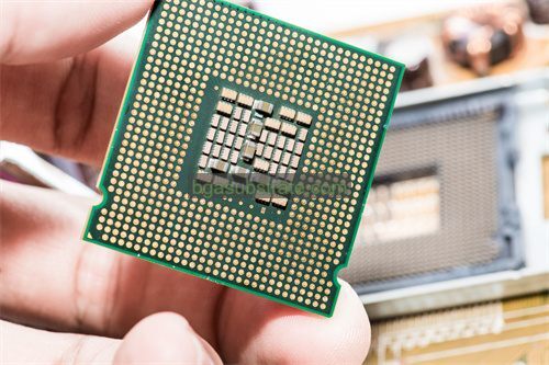
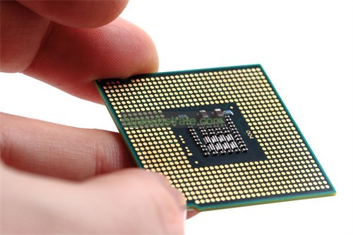
FCCSP (Fine-Pitch Chip Scale Package) substrate is a type of semiconductor packaging used for integrated circuits (ИС). It is a variant of chip scale packaging that offers a compact and high-density solution, particularly beneficial for applications where space and performance are critical.
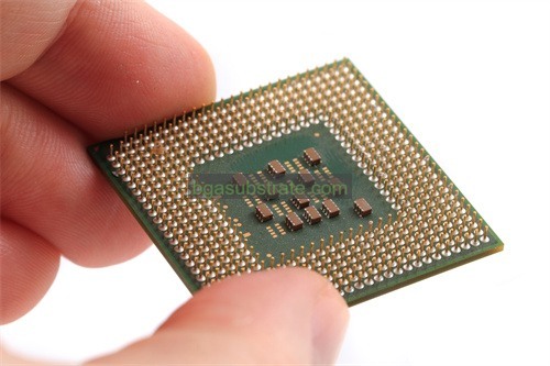
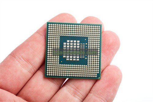
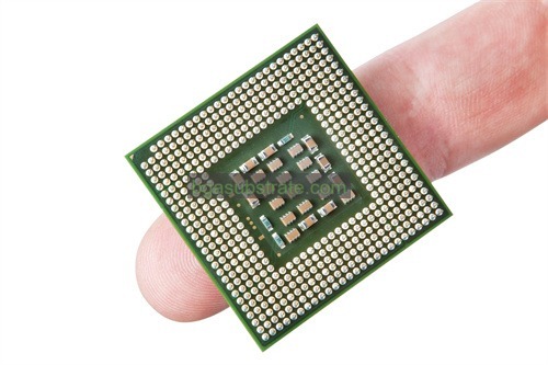
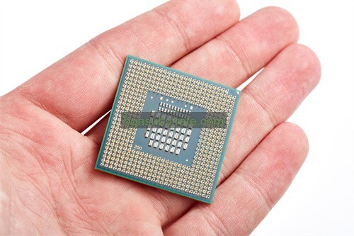
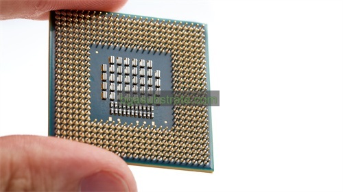
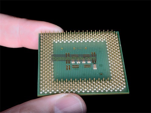
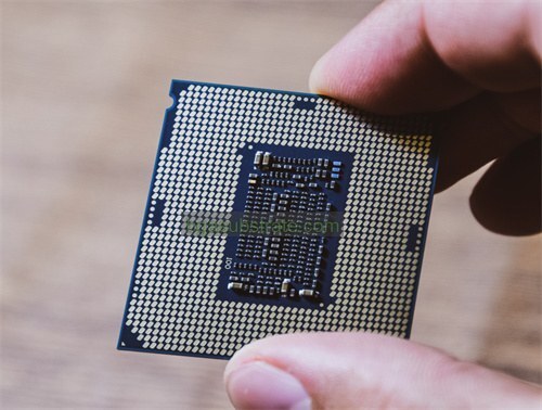
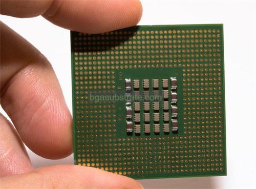
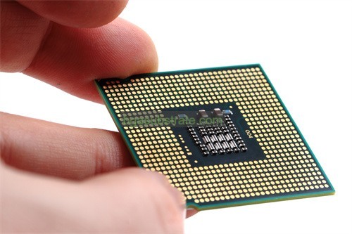
The FCCSP substrate typically features a fine-pitch ball grid array (BGA) structure, where solder balls are arranged in a grid pattern underneath the package, allowing for a higher density of connections compared to traditional packages. This configuration facilitates better electrical performance and thermal dissipation, which are crucial for high-speed and high-power ICs.
The substrate itself is often made from materials such as FR4 (a type of fiberglass epoxy laminate) or more advanced materials like BT (Bismaleimide-Triazine) resin, depending on the performance requirements. The choice of substrate material affects the thermal conductivity, механическая прочность, and electrical characteristics of the final package.
FCCSP substrates are designed with multiple layers to include signal routing, power distribution, and grounding planes, all of which contribute to the overall performance and reliability of the package. These layers are carefully engineered to ensure minimal signal interference and optimal thermal management.
Резюме, FCCSP substrates are crucial for modern electronics, providing a high-density, efficient, and reliable packaging solution that meets the demands of advanced semiconductor devices.

Производитель подложек FCCSP
Что такое FCCSP Substrate Рекомендации по проектированию?
FCCSP (Fine-Pitch Chip Scale Package) субстрат design guidelines are essential for ensuring the performance, надёжность, and manufacturability of the final semiconductor package. Вот некоторые ключевые соображения по проектированию:
- Substrate Material Selection: Choose appropriate substrate materials based on the thermal, механический, and electrical requirements of the application. Common materials include FR4, BT (Bismaleimide-Triazine) resin, and advanced ceramics, each offering different properties such as thermal conductivity and dielectric constant.
- Layer Stackup: Design the substrate with an optimal layer stackup to accommodate signal routing, power distribution, and grounding. Ensure that the stackup supports the necessary electrical performance and thermal management. Typically, the stackup includes layers for signal traces, power planes, and ground planes.
- Ball Grid Array (BGA) Layout: Plan the BGA layout carefully to accommodate the fine-pitch design. The spacing and placement of solder balls should be optimized to ensure reliable connections and avoid issues such as solder bridging or misalignment.
- Управление температурным режимом: Implement effective thermal management strategies to dissipate heat generated by the IC. This may involve using heat spreaders, thermal vias, or dedicated thermal pads to ensure the package operates within safe temperature limits.
- Signal Integrity:Maintain signal integrity by designing trace routings with appropriate widths and spacing. Minimize signal interference and crosstalk by following best practices for high-speed signal routing, including impedance control and proper grounding.
- Manufacturing Considerations: Design the substrate to be compatible with standard manufacturing processes, including etching, металлизация, and solder mask application. Ensure that the design allows for easy alignment and assembly during the production phase.
- Reliability Testing: Include design features that facilitate reliability testing, such as test pads or inspection areas. Perform thorough testing to identify potential issues related to thermal cycling, mechanical stress, and electrical performance.
Придерживаясь этих рекомендаций по проектированию, FCCSP substrates can achieve high performance and reliability, meeting the demanding requirements of modern semiconductor applications.
Преимущества FCCSP Substrate
FCCSP (Fine-Pitch Chip Scale Package) Субстратов offer several advantages that make them a popular choice in advanced semiconductor packaging. Here are some key benefits:
- Compact Size: FCCSP substrates are designed to be smaller and more compact than traditional packages. This fine-pitch, chip-scale approach reduces the overall footprint of the package, making it ideal for space-constrained applications.
- High Density: The fine-pitch ball grid array (BGA) layout used in FCCSP substrates allows for a higher density of connections. This enables more I/O pins in a smaller area, which is beneficial for high-performance ICs requiring numerous connections.
- Improved Electrical Performance: The design of FCCSP substrates includes optimized signal routing and reduced parasitics, which enhances electrical performance. This is particularly important for high-speed and high-frequency applications, where signal integrity is crucial.
- Enhanced Thermal Management: FCCSP substrates often incorporate features such as thermal vias or heat spreaders to improve thermal dissipation. This helps in managing the heat generated by the IC, contributing to better performance and longevity.
- Reduced Package Warping: The use of high-quality substrate materials and precise manufacturing processes in FCCSP substrates reduces the risk of package warping. This ensures better alignment and reliability during assembly and operation.
- Cost-Effective: Despite the advanced design, FCCSP substrates can be cost-effective compared to other high-density packaging options. Their compact size and efficient use of materials can lead to lower overall packaging costs.
- Manufacturing Compatibility: FCCSP substrates are compatible with standard manufacturing processes, making them easier to produce and assemble. This compatibility helps streamline production and reduce manufacturing complexities.
Резюме, FCCSP substrates offer a combination of compact size, high density, improved electrical and thermal performance, and cost-effectiveness, making them a valuable choice for modern semiconductor packaging needs.
Что такое FCCSP Substrate Процесс изготовления?
The FCCSP (Fine-Pitch Chip Scale Package) substrate fabrication process involves several critical steps to ensure the performance and reliability of the final package. Here’s an overview of the typical process:
- Design and Layout: The process begins with designing the FCCSP substrate layout. This involves defining the ball grid array (BGA) pattern, signal traces, power planes, and grounding planes. The design must consider electrical performance, Управление температурным режимом, и технологичность.
- Подготовка материала: Select and prepare substrate materials, which may include FR4, BT resin, or other advanced materials. The choice of material affects the thermal, механический, and electrical properties of the substrate.
- Photoresist Coating: Apply a photoresist layer onto the substrate material. This photoresist layer is used to define the areas that will be etched away during the manufacturing process. The coating ensures precise patterning for circuitry and other features.
- Photolithography: Use photolithography to transfer the substrate design onto the photoresist layer. This involves exposing the photoresist to ultraviolet (УЛЬТРАФИОЛЕТОВЫЙ) light through a photomask, which creates a pattern that corresponds to the desired circuitry and features.
- Офорт: Perform etching to remove the unprotected areas of the substrate material. This step creates the necessary circuitry and features on the substrate. Both wet and dry etching methods may be used, depending on the material and design requirements.
- Металлизация: Deposit metal layers onto the substrate to form electrical connections and features. Plating involves electroplating or chemical plating techniques to apply metal such as copper to the substrate, creating the necessary conductive paths.
- Via Formation: Create vias, or vertical interconnections, through the substrate layers. These vias connect different layers of the substrate and enable electrical connections between them. Techniques like laser drilling or mechanical drilling are used to form vias.
- Нанесение паяльной маски: Apply a solder mask to protect areas of the substrate where solder should not be applied. The solder mask also helps prevent solder bridging and short circuits during the assembly process.
- Ball Placement: Attach solder balls to the substrate’s BGA pattern. These solder balls serve as the electrical interface between the substrate and the printed circuit board (PCB) or other components. Placement accuracy is crucial to ensure reliable connections.
- Curing and Testing: Cure the substrate to solidify any applied materials and ensure proper adhesion. Conduct thorough testing to check for defects, Электрические характеристики, and reliability. This includes inspecting solder ball placement and checking for any manufacturing issues.
- Final Inspection and Packaging: Perform a final inspection to ensure the FCCSP substrate meets all design specifications and quality standards. Package the substrates for shipment or further assembly with semiconductor chips.
Резюме, the FCCSP substrate fabrication process involves a series of steps including design, material preparation, photoresist coating, photolithography, офорт, металлизация, via formation, Нанесение паяльной маски, ball placement, curing, testing, and final inspection. Each step is crucial for achieving the high performance and reliability required for fine-pitch chip scale packages.
Применение керамики FCCSP Substrate
Ceramic FCCSP (Fine-Pitch Chip Scale Package) substrates are used in various advanced electronic applications due to their superior properties. Вот некоторые ключевые области применения:
- High-Performance Computing: Ceramic FCCSP substrates are widely used in high-performance computing devices such as servers and processors. Their excellent thermal conductivity and electrical performance help manage heat dissipation and ensure stable operation of high-speed processors.
- Электросвязь: In telecommunications equipment, ceramic FCCSP substrates provide reliable performance for high-frequency signals and data transmission. Their low dielectric loss and high signal integrity make them ideal for use in RF (radio frequency) и микроволновые приложения.
- Электроника: Ceramic FCCSP substrates are utilized in consumer electronics like smartphones, Таблетки, and wearables. Their compact size and high density support the miniaturization of devices while maintaining high performance and reliability.
- Автомобильная электроника: In the automotive industry, ceramic FCCSP substrates are employed in various applications, including advanced driver assistance systems (АДАС), infotainment systems, and engine control units (Экю). Their robustness and thermal stability ensure reliable performance under harsh operating conditions.
- Аэрокосмическая и оборонная промышленность: The aerospace and defense sectors benefit from ceramic FCCSP substrates due to their high reliability and resistance to extreme temperatures and radiation. They are used in avionics, satellite systems, and other mission-critical applications where performance and durability are paramount.
- Медицинские приборы: Ceramic FCCSP substrates are used in medical devices and equipment due to their biocompatibility and stability. Applications include medical imaging systems, диагностическое оборудование, и имплантируемые устройства, where precision and reliability are essential.
- Силовая электроника: In power electronics, ceramic FCCSP substrates help manage heat and provide high reliability for power converters, inverters, and other power management systems. Their thermal conductivity and mechanical strength are crucial for handling high power levels and maintaining performance.
Резюме, ceramic FCCSP substrates are applied in a wide range of fields, including high-performance computing, электросвязь, Электроника, automotive systems, Аэрокосмическая и оборонная промышленность, Медицинские приборы, and power electronics. Their advantages, such as high thermal conductivity, Электрические характеристики, и механическая прочность, make them suitable for demanding and high-reliability applications.
Часто задаваемые вопросы о FCCSP Substrate
What are the advantages of FCCSP substrates?
FCCSP substrates offer a compact size, high density of connections, improved electrical performance, enhanced thermal management, reduced package warping, and cost-effectiveness.
What materials are used for FCCSP substrates?
Common materials include FR4 (fiberglass epoxy), BT resin (Bismaleimide-Triazine), and advanced ceramics. The choice depends on the specific requirements for thermal conductivity, Электрические характеристики, и механическая прочность.
How is the FCCSP substrate fabricated?
The fabrication process involves designing the substrate layout, applying photoresist, photolithography, офорт, металлизация, forming vias, applying solder masks, placing solder balls, and performing curing and testing.
What are the typical applications of FCCSP substrates?
FCCSP substrates are used in high-performance computing, электросвязь, Электроника, automotive systems, Аэрокосмическая и оборонная промышленность, Медицинские приборы, and power electronics.
What is the difference between FCCSP and other chip scale packages?
FCCSP offers a finer pitch ball grid array compared to some other chip scale packages, allowing for higher density and improved performance. It is designed to be more compact and provide better thermal and electrical characteristics.
How do FCCSP substrates handle heat?
FCCSP substrates are designed with features like thermal vias or heat spreaders to manage heat dissipation effectively, ensuring that the IC operates within safe temperature limits.
 Название вашего сайта


