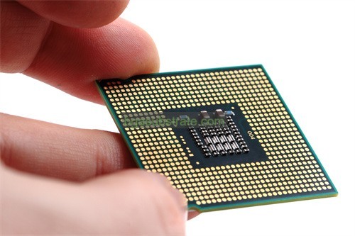
FCBGA Substrate Изготовитель
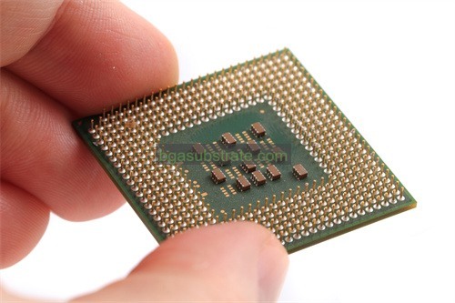
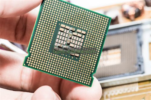
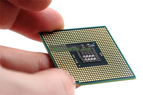
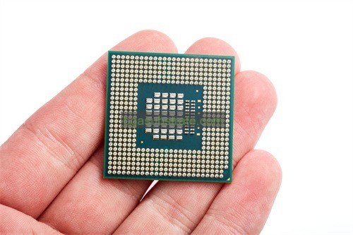
Производитель подложек FCBGA,FCBGA (Flip Chip Ball Grid Array) substrates are high-performance packaging solutions designed for flip chip technology, where the semiconductor chip is mounted face-down onto the substrate. This arrangement enables direct electrical connections through solder bumps, resulting in shorter interconnects and reduced signal latency. FCBGA substrates offer excellent thermal management and mechanical stability, making them ideal for high-power applications such as processors, GPUs, and other high-performance computing devices. The ball grid array configuration provides a dense array of electrical connections, supporting high pin counts and high-speed data transfer. FCBGA substrates are crucial for enabling compact, efficient, and reliable electronic packages in advanced technologies.
Что такое FCBGA Substrate?
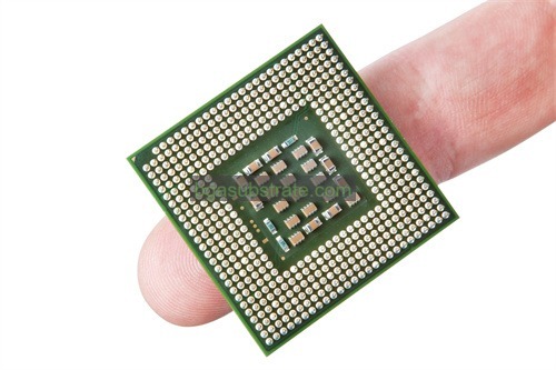
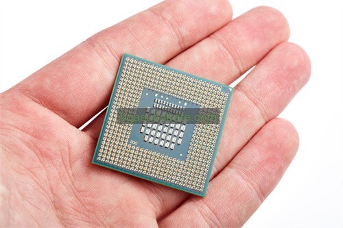
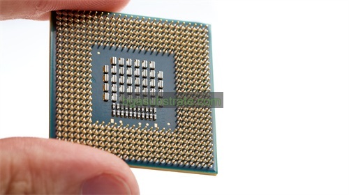
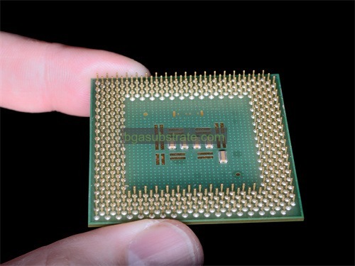
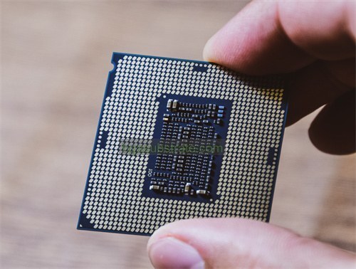
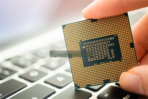
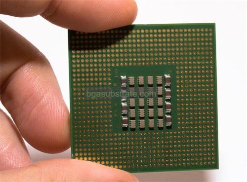
FCBGA (Flip Chip Ball Grid Array) substrates are crucial components in advanced electronic packaging, providing a foundation for high-performance integrated circuits. These substrates are used in Flip Chip Ball Grid Array packages, a type of packaging where the integrated circuit (IC) is mounted upside down, and the electrical connections are made via solder balls arranged in a grid pattern on the bottom of the package.
The primary role of an FCBGA substrate is to establish electrical and thermal connections between the IC and the circuit board. It achieves this through a multi-layered design that includes layers of conductive traces, dielectric materials, and often, embedded passive components. The substrate’s structure is designed to support the flip chip’s array of solder balls, which makes the package compact and efficient in terms of electrical performance and thermal management.
FCBGA substrates are known for their high-density interconnects and excellent thermal conductivity. They typically use advanced materials such as epoxy resin, polyimide, and high-performance ceramics to ensure reliability and performance. The design and material choices for FCBGA substrates are crucial in meeting the demands of high-speed, Высокочастотные приложения, as well as providing robust mechanical support for the IC.
Резюме, FCBGA substrates play a vital role in modern electronics by enabling efficient and reliable connections between ICs and their circuit boards. Their advanced design and material composition help address the challenges of high-density packaging and thermal management in cutting-edge electronic devices.

Производитель подложек FCBGA
Что такое FCBGA Substrate Рекомендации по проектированию?
Designing an FCBGA (Flip Chip Ball Grid Array) субстрат involves several critical considerations to ensure optimal performance, надёжность, и технологичность. Here are key guidelines for designing an FCBGA substrate:
- Layer Structure: The substrate typically comprises multiple layers, including signal layers, power/ground planes, and dielectric layers. Ensuring a well-defined layer stack-up is crucial for managing electrical performance and thermal dissipation.
- Ball Grid Array Layout: The arrangement and size of solder balls are fundamental. The grid should be designed to provide adequate mechanical support and electrical connectivity. Precision in ball placement is essential to avoid solder bridging and ensure reliable connections.
- Signal Integrity: To maintain high signal integrity, use controlled impedance traces and appropriate routing techniques. Pay attention to trace widths, интервал, and dielectric properties to minimize signal loss and crosstalk.
- Управление температурным режимом: Effective heat dissipation is vital for preventing overheating and ensuring reliable operation. Incorporate thermal vias, heat sinks, or thermal pads as needed to manage the heat generated by the IC.
- Material Selection: Choose high-quality materials for the substrate, such as low-loss dielectric materials and high-conductivity copper. The material should meet the electrical and thermal requirements of the application while also being compatible with the manufacturing processes.
- Manufacturing Constraints: Design with manufacturing capabilities in mind, including the minimum trace width, интервал, and via sizes that the fabrication process can achieve. This helps avoid potential issues during production and assembly.
- Reliability Testing: Plan for reliability testing, including thermal cycling, mechanical stress tests, and solder joint reliability assessments. These tests ensure that the substrate can withstand the operational and environmental stresses it will encounter.
- Design for Assembly: Ensure that the design is optimized for assembly processes, including soldering and inspection. Considerations should include pad sizes, solder mask clearances, and component alignment.
By adhering to these guidelines, designers can create FCBGA substrates that deliver high performance, надёжность, and manufacturability for advanced electronic applications.
Преимущества FCBGA Substrate
FCBGA (Flip Chip Ball Grid Array) Субстратов offer several significant advantages that make them a preferred choice in advanced electronic packaging:
- High I/O Density: FCBGA substrates support a high number of input/output (I/O) connections in a compact space. This high I/O density is achieved through the use of solder balls arranged in a grid pattern, which allows for efficient and reliable connections even in densely packed designs.
- Improved Electrical Performance: The flip chip design allows for shorter interconnect paths between the integrated circuit (IC) and the substrate. This reduces signal trace lengths and improves electrical performance by minimizing signal loss, crosstalk, and delay.
- Enhanced Thermal Management: FCBGA substrates typically incorporate multiple layers and advanced materials that enhance thermal conductivity. This helps in effective heat dissipation from the IC, reducing the risk of overheating and improving overall reliability.
- Reduced Package Size: The compact nature of FCBGA packaging allows for smaller overall package sizes compared to traditional packaging methods. This is beneficial for applications where space is limited, such as in mobile devices and portable electronics.
- Improved Reliability: The use of solder balls in FCBGA packages enhances mechanical robustness and solder joint reliability. The flip chip approach also reduces the risk of solder joint failures and improves the long-term durability of the package.
- Better Performance for High-Speed Applications: FCBGA substrates are well-suited for high-speed and high-frequency applications due to their low inductance and capacitance. This makes them ideal for demanding applications in telecommunications, computing, and data processing.
- Flexibility in Design: FCBGA substrates allow for greater design flexibility, including the integration of various components and functionalities within a single package. This flexibility supports the development of complex and advanced electronic systems.
- Экономичность: Although the initial cost of FCBGA substrates may be higher, their advantages in terms of performance, надёжность, and size often result in overall cost savings. This is particularly true for high-volume production where the benefits outweigh the initial investment.
Резюме, FCBGA substrates offer enhanced electrical and thermal performance, high I/O density, reduced package size, and improved reliability, making them a valuable choice for advanced electronic packaging needs.
Что такое FCBGA Substrate Процесс изготовления?
The fabrication of an FCBGA (Flip Chip Ball Grid Array) substrate involves a series of precise and intricate steps to ensure the final product meets the required performance and reliability standards. Here is an overview of the typical FCBGA substrate fabrication process:
- Design and Layout: The process begins with designing the substrate layout, including the arrangement of signal traces, power/ground planes, and the ball grid array pattern. The design is created using specialized electronic design automation (EDA) tools.
- Substrate Material Preparation: The substrate is usually made from high-performance materials such as epoxy resin, polyimide, или керамические. The base material is prepared and cut to the required size for the substrate.
- Layer Lamination: The substrate is built up in multiple layers. These layers, including signal layers, dielectric layers, and power/ground planes, are laminated together using heat and pressure. This creates a multi-layered structure necessary for high-density interconnects.
- Photolithography: A photolithographic process is used to define the circuit patterns on the substrate. This involves applying a photosensitive layer (photoresist) to the substrate, exposing it to light through a mask, and then developing the exposed photoresist to create the desired pattern.
- Офорт: After photolithography, the exposed areas of the substrate are etched away to remove unwanted copper or other conductive materials, leaving behind the desired circuit patterns. This process can be either wet etching or dry etching, depending on the materials and design requirements.
- Via Formation: Vias, which are vertical electrical connections between different layers of the substrate, are created using drilling and plating processes. The vias are filled with metal to establish electrical connections between the different layers.
- Solder Mask and Surface Finish: A solder mask layer is applied to protect areas of the substrate where solder is not desired. Дополнительно, a surface finish is applied to the pads where solder balls will be attached. Common surface finishes include electroplated gold, immersion silver, или OSP (Органический консервант для пайки).
- Ball Grid Array Assembly: Solder balls are precisely placed in the designated grid pattern on the substrate. These balls serve as the electrical connections between the substrate and the PCB or other mounting surfaces. The solder balls are typically attached using a reflow soldering process, where the substrate is heated to melt and attach the solder balls.
- Инспекция и тестирование: The finished FCBGA substrates undergo rigorous inspection and testing to ensure they meet quality standards. This includes visual inspections, electrical tests, and reliability assessments such as thermal cycling and mechanical stress tests.
- Cutting and Packaging: Наконец, the substrates are cut into individual units and packaged for delivery. This stage ensures that the FCBGA substrates are ready for integration into electronic assemblies and systems.
Резюме, the FCBGA substrate fabrication process involves meticulous design, layering, photolithography, офорт, via formation, and ball grid array assembly. Each step is critical to achieving high performance and reliability in the final substrate.
Применение керамики FCBGA Substrate
Ceramic FCBGA (Flip Chip Ball Grid Array) substrates are highly valued in various advanced electronic applications due to their superior properties and performance. Here are key applications where ceramic FCBGA substrates are utilized:
- High-Performance Computing: Ceramic FCBGA substrates are widely used in high-performance computing systems, including servers and workstations. Their excellent thermal conductivity and electrical performance make them ideal for handling the high speeds and power densities required by modern processors and memory modules.
- Электросвязь: In telecommunications equipment, such as base stations and network infrastructure, ceramic FCBGA substrates provide reliable performance for high-speed data transmission. Their ability to manage heat and maintain signal integrity is crucial for ensuring efficient operation in communication systems.
- Электроника: Ceramic FCBGA substrates are found in high-end consumer electronics, including smartphones, Таблетки, и игровые консоли. Their compact size, high I/O density, and thermal management capabilities help in designing smaller, more powerful devices with enhanced performance.
- Автомобильная электроника: The automotive industry benefits from ceramic FCBGA substrates in applications such as advanced driver assistance systems (АДАС) and engine control units (Экю). Their durability and thermal stability are essential for withstanding the harsh conditions and high temperatures encountered in automotive environments.
- Аэрокосмическая и оборонная промышленность: In aerospace and defense applications, where reliability and performance are critical, ceramic FCBGA substrates are used in avionics, Радиолокационные системы, and other mission-critical electronics. Their ability to operate reliably under extreme conditions and high-frequency applications makes them suitable for these demanding environments.
- Медицинские приборы: Ceramic FCBGA substrates are employed in high-precision medical devices, including imaging systems and diagnostic equipment. Their reliability, Электрические характеристики, and resistance to environmental factors contribute to the accuracy and durability of medical technologies.
- Industrial Electronics: In industrial automation and control systems, ceramic FCBGA substrates are used to support high-speed data processing and robust performance. Their ability to handle high temperatures and maintain signal integrity is advantageous for demanding industrial applications.
- RF and Microwave Applications: Ceramic FCBGA substrates are well-suited for RF (Радиочастота) and microwave applications due to their low dielectric loss and high thermal conductivity. They are used in RF components, such as amplifiers and filters, where performance at high frequencies is essential.
Резюме, ceramic FCBGA substrates are integral to a wide range of applications due to their superior thermal management, Электрические характеристики, and durability. Their use spans across high-performance computing, электросвязь, Электроника, автомобильный, аэрокосмический, Медицинские приборы, industrial electronics, and RF/microwave applications.
Часто задаваемые вопросы о FCBGA Substrate
What are the main advantages of FCBGA substrates?
FCBGA substrates offer high I/O density, improved electrical performance, enhanced thermal management, reduced package size, and increased reliability. They are well-suited for high-speed, high-performance applications.
How does the FCBGA substrate improve electrical performance?
The flip chip design minimizes the length of signal paths between the IC and the substrate, reducing signal loss, crosstalk, and delay. This results in better electrical performance compared to traditional packaging methods.
What materials are used in FCBGA substrates?
FCBGA substrates are typically made from materials such as epoxy resin, polyimide, or ceramics. These materials are chosen for their electrical and thermal properties to ensure high performance and reliability.
What is the role of solder balls in FCBGA substrates?
Solder balls are used to create electrical and mechanical connections between the IC and the circuit board. They are arranged in a grid pattern on the bottom of the package, facilitating a compact and efficient connection.
What are common applications for FCBGA substrates?
FCBGA substrates are used in high-performance computing, электросвязь, Электроника, Автомобильная электроника, Аэрокосмическая и оборонная промышленность, Медицинские приборы, industrial electronics, and RF/microwave applications.
How is an FCBGA substrate fabricated?
The fabrication process involves several steps, including designing the layout, preparing and laminating substrate materials, photolithography, офорт, forming vias, applying solder mask and surface finish, placing solder balls, and finally inspecting and testing the substrate.
 Название вашего сайта

