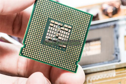
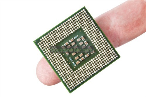
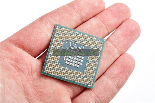
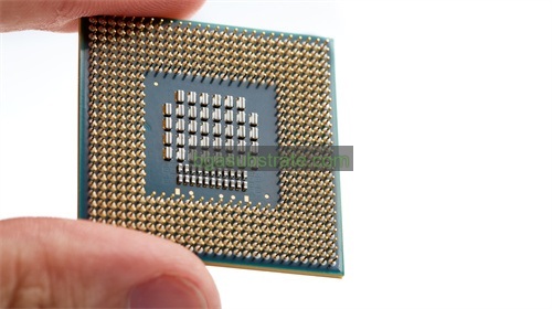
TU-872 SLK Substrate Manufacturer
TU-872 SLK Substrate Manufacturer,TU-872 SLK substrate is a high-performance laminate designed for sophisticated electronic applications, particularly in the RF and microwave domains. It features a low dielectric constant and low loss tangent, ensuring excellent signal integrity and minimal signal degradation. The substrate is engineered for high thermal stability and low moisture absorption, which enhance its reliability in harsh environments. Its compatibility with fine-line processing allows for high-density interconnect designs, making it suitable for multilayer circuit boards. TU-872 SLK is commonly used in telecommunications, aerospace, and automotive sectors, where precision and performance are critical for advanced electronic systems.
What is TU-872 SLK Substrate?
TU-872 SLK substrate is a high-performance multilayer circuit board material widely used in the electronics industry, especially in applications that require high standards, such as RF (radio frequency) and microwave devices. This substrate is known for its superior electrical properties, thermal stability, and mechanical strength, making it suitable for high-speed signal transmission and high-frequency applications.
The main features of TU-872 SLK substrate include a low dielectric constant and low dielectric loss, which effectively reduce signal attenuation and enhance transmission efficiency. Additionally, this material maintains excellent performance in high-temperature environments, ensuring outstanding results under harsh working conditions. Its thermal resistance and moisture resistance contribute to long-term reliability and stability, making it suitable for high-end electronic devices such as satellite communications, radar systems, and wireless communication base stations.
During the manufacturing process, TU-872 SLK substrate undergoes precise processing, meeting the demands of high-density interconnect (HDI) design, which supports microvias and complex circuitry. This allows designers to achieve higher functional integration in limited space, driving the miniaturization and lightweight nature of electronic products.
In summary, TU-872 SLK substrate has become an essential material in high-frequency electronic applications due to its excellent electrical and mechanical properties, supporting the advancement of modern electronic technology.

TU-872 SLK Substrate Manufacturer
What is the TU-872 SLK Substrate Design Guidelines?
The design guidelines for TU-872 SLK substrates focus on optimizing performance and manufacturability. Here are some key points:
- Layer Stack-Up: Define the appropriate number of layers based on the circuit complexity. Ensure that signal layers are placed effectively to minimize interference.
- Trace Width and Spacing: Follow standard guidelines for trace width and spacing to maintain impedance control, especially for high-frequency signals. Use appropriate calculators to determine these values based on the substrate thickness and dielectric properties.
- Vias: Utilize microvias for high-density interconnections. Ensure proper plating and aspect ratio to maintain signal integrity.
- Impedance Control: Design traces with controlled impedance by considering the dielectric thickness, width, and the overall geometry of the stack-up. Simulation tools can be beneficial for accurate impedance analysis.
- Thermal Management: Design for adequate thermal dissipation. Consider placing thermal vias and ground planes appropriately to manage heat in high-power applications.
- Clearances and Dimensions: Adhere to manufacturer specifications for minimum clearance and dimensions to ensure reliable fabrication and assembly.
- Testing Points: Include test pads and points for electrical testing during manufacturing, which can aid in identifying defects early.
- Signal Integrity: Use simulation tools to analyze signal integrity, particularly for high-speed designs, to minimize issues such as ringing and crosstalk.
- Material Considerations: Ensure that any components used are compatible with the thermal and mechanical properties of the TU-872 SLK substrate.
By following these guidelines, designers can maximize the performance and reliability of circuits built on TU-872 SLK substrates.
The advantages of TU-872 SLK Substrate
The TU-872 SLK substrate offers several advantages that make it an excellent choice for high-performance electronic applications:
- Low Dielectric Loss: Its low dielectric loss ensures minimal signal attenuation, which is crucial for high-frequency and RF applications.
- High Thermal Stability: TU-872 SLK maintains performance under elevated temperatures, making it suitable for environments with significant thermal fluctuations.
- Excellent Electrical Properties: The substrate features a low dielectric constant, which helps in maintaining signal integrity and reducing crosstalk.
- Mechanical Strength:It possesses high mechanical strength, providing durability and reliability in various applications, including those subjected to physical stress.
- Compatibility with HDI Designs: The substrate supports high-density interconnect (HDI) designs, allowing for microvias and complex circuit layouts that enhance functionality within limited space.
- Good Moisture Resistance: TU-872 SLK is resistant to moisture, ensuring long-term stability and reliability, particularly in humid environments.
- Thermal Management: Effective thermal management properties enable better heat dissipation, which is essential for high-power applications.
- Easy Fabrication: The material is amenable to standard PCB fabrication processes, facilitating efficient manufacturing and assembly.
These advantages make TU-872 SLK an ideal choice for advanced electronic devices, including satellite communications, radar systems, and wireless communication technologies.
What is the TU-872 SLK Substrate Fabrication Process?
The fabrication process for TU-872 SLK substrates typically involves several key steps to ensure high-quality performance and precision. Here’s an overview:
- Material Preparation: The raw TU-872 SLK material is sourced and cut into sheets of the required size. Quality control checks are conducted to ensure consistency.
- Layer Design: Design files are created based on the desired circuit layout, including layer stack-up and trace routing. This includes defining electrical specifications and impedance requirements.
- Photolithography: A photomask is created based on the design, and a photoresist layer is applied to the substrate. UV light exposes the photoresist, transferring the circuit pattern onto the substrate.
- Etching: The exposed areas of the substrate are etched away using chemical etching processes to create the desired circuit traces and pads.
- Via Drilling: Microvias and through-holes are drilled using laser or mechanical drilling techniques, depending on the design specifications.
- Plating: The drilled vias are plated with copper to ensure electrical connectivity. This process can include electroless and electrolytic plating.
- Surface Finishing:Surface finishes such as immersion gold, ENIG (Electroless Nickel Immersion Gold), or other finishes are applied to enhance solderability and corrosion resistance.
- Layer Lamination: For multilayer designs, layers are stacked and laminated under heat and pressure to bond them together securely.
- Final Etching and Cleaning: Any remaining photoresist is removed, and final etching is done to ensure all traces are correctly formed. The substrate is then cleaned to remove any residues.
- Testing: Electrical testing is performed to verify the integrity of the circuits, ensuring there are no defects or shorts.
- Final Inspection:A thorough inspection process is conducted to ensure that all specifications and quality standards are met before shipment.
This process ensures that TU-872 SLK substrates are manufactured to high standards, suitable for demanding applications in RF and microwave electronics.
The application of ceramic TU-872 SLK Substrate
The ceramic TU-872 SLK substrate is used in various high-performance applications due to its excellent electrical and thermal properties. Key applications include:
- RF and Microwave Devices: Its low dielectric loss and high thermal stability make it ideal for RF amplifiers, mixers, and oscillators.
- Satellite Communications: The substrate’s reliability under harsh environmental conditions is crucial for satellite transponders and communication systems.
- Aerospace Electronics: TU-872 SLK substrates are used in aerospace applications where high performance and durability are essential.
- Medical Devices: In medical imaging and diagnostic equipment, the substrate’s precision and signal integrity enhance device functionality.
- Telecommunications:It is employed in base stations and wireless communication devices for improved signal clarity and reduced interference.
- Automotive Applications: Used in advanced driver-assistance systems (ADAS) and other high-frequency automotive electronics, ensuring reliable performance.
These applications leverage the substrate’s unique properties, contributing to the advancement of modern electronic technologies.
FAQs about TU-872 SLK Substrate
What is TU-872 SLK substrate made of?
TU-872 SLK is a ceramic substrate known for its low dielectric loss and excellent thermal stability, making it suitable for high-frequency applications.
What are the key advantages of using TU-872 SLK?
Key advantages include low dielectric constant, high thermal stability, excellent electrical properties, mechanical strength, and compatibility with high-density interconnect (HDI) designs.
What applications are best suited for TU-872 SLK substrates?
It is widely used in RF and microwave devices, satellite communications, aerospace electronics, medical devices, telecommunications, and automotive applications.
How is the fabrication process for TU-872 SLK substrate conducted?
The fabrication involves material preparation, photolithography, etching, via drilling, plating, surface finishing, layer lamination, testing, and final inspection.
Can TU-872 SLK substrates support high-frequency signals?
Yes, TU-872 SLK substrates are specifically designed to support high-frequency signals with minimal signal loss and interference.
Is TU-872 SLK substrate compatible with standard PCB manufacturing processes?
Yes, it can be integrated into standard PCB fabrication processes, facilitating efficient manufacturing and assembly.
What types of surface finishes are recommended for TU-872 SLK substrates?
Common surface finishes include ENIG (Electroless Nickel Immersion Gold) and other finishes that enhance solderability and corrosion resistance.
What testing is performed on TU-872 SLK substrates?
Electrical testing is conducted to verify circuit integrity, ensuring that there are no defects or shorts before the substrate is shipped.
 Your Website Name

