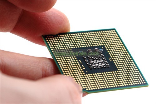
108 Layer PCB Manufacturer
108 Layer PCB Manufacturer,A 108-layer PCB is an advanced circuit board featuring an impressive 108 layers of conductive and insulating materials. This high-density multilayer design enables complex and compact circuit configurations, allowing for intricate electronic systems with extensive functionality. The numerous layers facilitate a large number of interconnections, which are essential for high-performance applications requiring dense circuitry and efficient signal routing. 108-layer PCBs are typically used in cutting-edge technology sectors such as aerospace, high-performance computing, and advanced telecommunications. Their ability to integrate a vast amount of circuitry in a compact form factor while maintaining high signal integrity and thermal management makes them crucial for sophisticated electronic systems.
What is 108 Layer PCB?
A 108-layer PCB (Printed Circuit Board) is a highly advanced circuit board with an exceptional number of layers, which is significantly higher than typical PCBs used in most applications. These PCBs are used in sophisticated electronic systems that demand high density, high performance, and extensive functionality, such as in aerospace, telecommunications, high-end computing, and advanced medical devices.
The construction of a 108-layer PCB involves stacking and interconnecting multiple layers of conductive and insulating materials. Each layer typically consists of a copper layer (used for circuit traces) and an insulating layer (such as FR4 or advanced materials like BT resin or prepreg). The layers are meticulously aligned and bonded together to create a compact and complex circuit.
The primary advantage of a 108-layer PCB is its ability to accommodate a large number of circuits in a relatively small form factor. This is achieved by stacking numerous layers of circuitry, which can greatly enhance the performance of the device by reducing signal interference, minimizing noise, and improving overall signal integrity. Such high-layer-count PCBs also allow for more efficient routing of connections, which is crucial for high-speed digital circuits and high-frequency applications.
Manufacturing a 108-layer PCB requires precise fabrication techniques, advanced materials, and sophisticated design tools. The process involves detailed planning to ensure that all layers are correctly aligned and that the electrical performance meets stringent specifications. As a result, 108-layer PCBs are typically more expensive and complex to produce compared to lower-layer count boards, but they are indispensable for high-performance and high-reliability electronic applications.

ISOLA 185HR Substrate Manufacturer
What is the 108 Layer PCB Design Guidelines?
Designing a 108-layer PCB requires meticulous planning and adherence to specific guidelines to ensure high performance and reliability. Here are some essential design guidelines for a 108-layer PCB:
- Layer Stack-Up Design: Carefully design the layer stack-up to achieve the desired electrical performance and mechanical stability. This includes defining the order and thickness of the signal, power, and ground layers. Ensure that the stack-up supports controlled impedance and minimizes signal interference.
- Signal Integrity: Use advanced signal integrity techniques such as differential signaling, proper trace routing, and impedance matching to maintain high signal quality. Pay close attention to high-speed signal layers and ensure proper trace impedance throughout the PCB.
- Thermal Management: With such a high number of layers, effective thermal management is crucial. Implement thermal vias, heat spreaders, and proper placement of heat-sensitive components to dissipate heat efficiently and prevent thermal issues.
- Power Distribution Network (PDN): Design an effective power distribution network to provide stable and noise-free power to the components. Use multiple power and ground planes to reduce power noise and ensure sufficient current handling capacity.
- Via and Hole Management: Minimize the use of through-hole vias to reduce signal degradation and impedance discontinuities. Consider using blind or buried vias where appropriate to optimize the signal routing and reduce electrical noise.
- Layer-to-Layer Routing: Ensure that the routing between different layers is optimized to prevent crosstalk and maintain signal integrity. Use appropriate routing techniques and keep sensitive signals away from noisy layers.
- Design for Manufacturing (DFM): Adhere to manufacturing guidelines and constraints to ensure that the PCB can be produced efficiently and with high quality. This includes considerations for drill sizes, pad sizes, and layer alignment.
- Simulation and Testing: Use simulation tools to model the electrical performance of the PCB and verify the design before fabrication. Conduct thorough testing, including electrical, thermal, and mechanical tests, to ensure that the final product meets all specifications.
By following these design guidelines, you can effectively manage the complexity of a 108-layer PCB and ensure that it performs reliably in demanding applications.
The advantages of 108 Layer PCB
A 108-layer PCB offers several significant advantages due to its complex design and high-density capabilities. Here are some key benefits:
- High-Density Integration: One of the primary advantages of a 108-layer PCB is its ability to accommodate a large number of circuits within a compact form factor. This high-density integration allows for the integration of more components and functionalities in a smaller space, which is essential for advanced electronic systems.
- Improved Signal Integrity: The use of multiple layers helps in reducing signal interference and noise. With proper layer stack-up and routing, a 108-layer PCB can achieve superior signal integrity, which is crucial for high-speed and high-frequency applications.
- Enhanced Power Distribution: A high layer count allows for a robust power distribution network with dedicated layers for power and ground. This results in improved power delivery, reduced voltage drops, and minimized noise, which enhances the overall reliability of the circuit.
- Thermal Management: Advanced thermal management solutions can be implemented in a 108-layer PCB. The multiple layers allow for efficient heat dissipation through thermal vias and heat spreaders, which helps in maintaining the thermal stability of high-power components.
- Reduced Crosstalk: With a well-designed layer stack-up, a 108-layer PCB can effectively manage crosstalk between different signal layers. This is achieved by carefully placing ground and power planes between signal layers, which helps in isolating sensitive signals and reducing interference.
- Improved Routing Flexibility: The extensive number of layers provides greater flexibility in routing complex interconnections. This allows designers to optimize signal paths and minimize the need for extensive external connections, leading to a more compact and efficient design.
- Enhanced Reliability: High-layer count PCBs are often used in critical applications where reliability is paramount. The design allows for redundancy and robust electrical performance, which enhances the overall reliability of the electronic system.
- Advanced Functionality:A 108-layer PCB can support advanced functionalities and features that are essential for modern high-performance systems, such as advanced communication protocols, high-speed data processing, and complex analog and digital circuitry.
These advantages make a 108-layer PCB an ideal choice for demanding applications in fields such as telecommunications, aerospace, defense, and high-end computing.
What is the 108 Layer PCB Fabrication Process?
The fabrication process for a 108-layer PCB is intricate and involves several detailed steps to ensure precision and reliability. Here’s an overview of the key steps involved in fabricating a 108-layer PCB:
- Design and Planning: The process begins with detailed design and planning, where the PCB layout, layer stack-up, and material specifications are defined. Advanced design tools are used to create a detailed schematic and layout, including the definition of the 108 layers.
- Material Preparation: High-quality base materials such as copper foil and prepreg (pre-impregnated fiberglass) are selected. The materials are prepared according to the specified layer requirements, including the thickness and type of insulating layers.
- Layer Fabrication:Each layer of the PCB is fabricated individually. This involves applying a photoresist layer on copper-clad laminates, exposing it to UV light through a photomask, and developing the exposed areas. The unwanted copper is then etched away, leaving behind the circuit pattern.
- Layer Registration: After the individual layers are fabricated, they are carefully aligned and registered. This involves precise alignment to ensure that all layers will stack correctly and that the circuitry will match across layers.
- Lamination: The registered layers are then laminated together under heat and pressure to form a single cohesive board. This step involves placing the layers in a press and applying heat and pressure to bond them together with an adhesive resin.
- Drilling: Vias and holes are drilled through the laminated stack using high-precision drilling equipment. This step is critical for creating the electrical connections between different layers of the PCB.
- Plating and Imaging: After drilling, the holes are plated with copper to form conductive pathways. The board is then imaged and additional photoresist is applied to define patterns for further etching and plating.
- Etching and Plating: The board undergoes etching to remove unwanted copper and plating to deposit additional copper where needed. This step refines the circuit patterns and ensures proper electrical connections.
- Surface Finish: A surface finish is applied to protect the copper and ensure good solderability. Common finishes include HASL (Hot Air Solder Leveling), ENIG (Electroless Nickel Immersion Gold), or other advanced finishes depending on the application requirements.
- Testing and Inspection: The completed PCB undergoes rigorous testing and inspection to ensure that it meets all design specifications and performance criteria. This includes electrical testing, visual inspection, and mechanical checks.
- Cutting and Profiling: The finished PCB is cut and profiled to the required dimensions. Any additional features, such as mounting holes or cutouts, are also created during this step.
- Assembly: If required, the PCB is assembled with components, which involves soldering components onto the board using techniques such as SMT (Surface Mount Technology) or through-hole soldering.
The fabrication of a 108-layer PCB is a highly complex process that requires precise control at every stage to ensure the final product meets the high standards required for advanced electronic applications.
The application of ceramic 108 Layer PCB
Ceramic 108-layer PCBs are utilized in specialized applications where their advanced properties are essential. Here are some key applications of ceramic 108-layer PCBs:
- High-Frequency and Microwave Applications: Ceramic 108-layer PCBs are ideal for high-frequency and microwave circuits due to their low dielectric loss and stable electrical characteristics. They are used in communication systems, radar, and satellite technology where high signal integrity and minimal signal attenuation are critical.
- Aerospace and Defense: In aerospace and defense applications, reliability and performance are paramount. Ceramic 108-layer PCBs are used in avionics systems, missile guidance systems, and military communication equipment. Their ability to handle high power and operate reliably in extreme conditions makes them suitable for these demanding environments.
- Medical Devices: Advanced medical devices, such as imaging equipment (MRI, CT scanners) and diagnostic tools, benefit from the high precision and reliability offered by ceramic 108-layer PCBs. These PCBs help ensure accurate signal transmission and minimal interference in sensitive medical electronics.
- High-Power Electronics: Ceramic PCBs are used in high-power applications where thermal management and electrical performance are critical. Examples include power amplifiers and high-power RF (radio frequency) devices. The ceramic material’s excellent thermal conductivity helps in efficient heat dissipation.
- Automotive Electronics: In the automotive industry, ceramic 108-layer PCBs are used in advanced driver assistance systems (ADAS), infotainment systems, and electric vehicle control units. Their durability and performance under varying temperatures and mechanical stresses are well-suited for automotive applications.
- High-Speed Computing: High-performance computing systems, including servers and supercomputers, use ceramic 108-layer PCBs to manage complex and high-speed signal routing. These PCBs help achieve the high data transfer rates and reliability required in data centers and high-speed computing environments.
- Telecommunications: In telecommunications infrastructure, such as base stations and networking equipment, ceramic 108-layer PCBs are employed to support high-speed data transmission and signal processing. Their stable electrical properties and reliability ensure efficient operation of communication systems.
- Consumer Electronics: While less common, ceramic 108-layer PCBs can also be found in high-end consumer electronics, such as high-resolution displays and advanced audio equipment. Their ability to handle high signal frequencies and reduce interference contributes to superior performance in these devices.
Overall, the use of ceramic 108-layer PCBs in these applications leverages their superior electrical, thermal, and mechanical properties to meet the demanding requirements of high-performance and high-reliability electronic systems.
FAQs about 108 Layer PCB
Why are 108-layer PCBs used?
They are used in advanced electronic systems where high-density integration, improved signal integrity, and enhanced power distribution are crucial. Applications include aerospace, medical devices, high-speed computing, and telecommunications.
What are the benefits of a 108-layer PCB?
Benefits include compact size, improved signal integrity, better power distribution, enhanced thermal management, and reduced crosstalk.
How is a 108-layer PCB fabricated?
The fabrication involves designing the layout, preparing materials, fabricating individual layers, aligning and laminating layers, drilling, plating, and applying surface finishes.
What materials are used in a 108-layer PCB?
Common materials include copper for conductive layers, prepreg and core materials for insulation, and ceramics or advanced laminates for specific performance requirements.
What challenges are associated with 108-layer PCBs?
Challenges include complex design and manufacturing processes, higher costs, and the need for precise alignment and testing.
How does thermal management work in a 108-layer PCB?
Thermal management is achieved through the use of thermal vias, heat spreaders, and proper layer stack-up to ensure efficient heat dissipation and maintain thermal stability.
 Your Website Name

