
Taconic PCB 생산자
타코닉 PCB 제조업체,Taconic PCBs are advanced circuit boards made from Taconic materials, which are renowned for their exceptional electrical and thermal properties. Taconic substrates, often composed of PTFE (폴리테트라플루오로에틸렌) and other high-performance materials, offer low dielectric loss and high-frequency stability, making them ideal for RF and microwave applications. These PCBs excel in maintaining signal integrity and minimizing signal degradation, even at high frequencies. They are widely used in telecommunications, 항공 우주, and high-speed digital circuits where reliability and performance are crucial. The combination of high thermal stability, 내화학성, and superior electrical characteristics makes Taconic PCBs a top choice for demanding electronic systems.
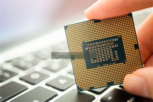
무엇입니까 Taconic PCB?
Taconic PCB refers to a type of printed circuit board (폴리염화비페) that utilizes Taconic’s specialized materials, which are known for their high-performance properties. Taconic is a leading manufacturer of advanced substrate materials, particularly those used in high-frequency and high-speed electronic applications.
Taconic PCBs typically employ materials such as PTFE (폴리테트라플루오로에틸렌) and ceramic-filled PTFE composites. These materials are renowned for their excellent dielectric properties, low loss tangents, and high thermal stability. They are particularly useful in applications requiring high-frequency signal transmission, such as microwave and RF (무선 주파수) circuits.
The key advantages of Taconic PCBs include their superior electrical performance, which is crucial for maintaining signal integrity and reducing signal loss. The low dielectric constant and loss tangent of Taconic materials help in minimizing signal degradation, making them ideal for high-speed digital and RF applications.
또한, Taconic PCBs offer high thermal conductivity and stability, ensuring reliable performance in demanding environments. The materials used can handle high power levels and are resistant to temperature fluctuations, which is important for maintaining PCB performance under various operational conditions.
전반적, Taconic PCBs are a preferred choice for applications in telecommunications, 항공 우주, and high-speed computing due to their advanced material properties and reliability in high-frequency scenarios.

타코닉 PCB 제조업체
무엇입니까 Taconic PCB 디자인 지침?
Taconic PCB Design Guidelines are a set of best practices and recommendations tailored to ensure optimal performance and reliability when designing printed circuit boards using Taconic’s advanced substrate materials. These guidelines address the unique properties of Taconic materials, such as PTFE (폴리테트라플루오로에틸렌) and ceramic-filled PTFE composites, which are known for their high-frequency and high-speed capabilities.
- 재료 선택: Choose the appropriate Taconic material based on the specific application requirements. For high-frequency applications, materials with low dielectric constants and loss tangents are essential. Taconic’s materials are designed to provide excellent signal integrity and minimal signal loss.
- 레이어 스택업(Layer Stack-Up): Design the PCB stack-up with careful consideration of the dielectric thickness and material properties. The stack-up should be optimized to balance impedance control, 신호 무결성, and thermal management. Ensure that the dielectric layers are consistent and properly aligned to maintain signal performance.
- 임피던스 제어: Pay close attention to impedance control when designing traces and signal paths. Use appropriate trace widths and spacing to achieve the desired impedance. Taconic materials offer precise impedance control, but it is crucial to model and verify the impedance using simulation tools.
- 열 관리: Consider thermal management strategies to handle heat dissipation effectively. Taconic materials have high thermal conductivity, which helps in managing heat, but ensure that the PCB design includes sufficient thermal vias and heat sinks where necessary.
- 신호 무결성: Implement design techniques to minimize signal degradation and noise. This includes careful routing of high-speed signals, proper grounding, and minimizing signal reflections. Use ground planes and shielding to enhance signal integrity and reduce electromagnetic interference (EMI (이엠아이)).
- Manufacturing Considerations: Follow best practices for manufacturing and assembly processes specific to Taconic materials. Ensure compatibility with standard fabrication techniques and verify that the design adheres to the material’s handling and processing requirements.
- 테스트 및 검증: Perform thorough testing and validation of the PCB design to ensure that it meets performance specifications. Use simulation tools to model the PCB behavior and conduct physical testing to verify the design under real-world conditions.
이 지침을 준수함으로써, designers can leverage the advanced properties of Taconic PCB materials to create high-performance and reliable circuit boards for demanding applications.
의 장점 Taconic PCB
Taconic PCBs offer several distinct advantages due to the advanced properties of the materials used in their construction. 주요 이점은 다음과 같습니다:
- Superior Electrical Performance: Taconic materials, such as PTFE (폴리테트라플루오로에틸렌) and ceramic-filled PTFE composites, provide excellent electrical performance. Their low dielectric constants and loss tangents help minimize signal degradation and signal loss, making them ideal for high-frequency and high-speed applications.
- High Thermal Stability: Taconic PCBs are known for their high thermal stability and conductivity. This property allows them to effectively manage heat, maintaining reliable performance even in demanding thermal environments. The materials are designed to withstand high temperatures without degrading, ensuring long-term reliability.
- 임피던스 제어: The advanced materials used in Taconic PCBs offer precise impedance control, which is crucial for maintaining signal integrity in high-speed and high-frequency circuits. This ensures consistent performance and reduces signal reflections and distortions.
- Low Signal Loss: Taconic substrates have low signal loss characteristics, which is essential for high-speed digital and RF (무선 주파수) 응용 프로그램. The low loss tangent of Taconic materials helps in preserving signal quality and achieving better overall system performance.
- 전자기 간섭 감소 (EMI (이엠아이)): The materials used in Taconic PCBs provide effective shielding against electromagnetic interference. This reduces noise and improves the overall performance of electronic systems, particularly in sensitive RF applications.
- 내구성 향상: Taconic materials are known for their durability and resistance to mechanical stress. This contributes to the longevity and robustness of the PCB, even in challenging operational conditions.
- Consistency and Reliability:Taconic’s manufacturing processes ensure that their materials maintain consistent properties across different production runs. This consistency helps in achieving reliable and repeatable performance in electronic applications.
- Versatility: Taconic PCBs can be used in a wide range of applications, 통신 포함, 항공 우주, and automotive industries. Their versatile properties make them suitable for various high-performance and high-reliability applications.
전반적, Taconic PCBs are valued for their high-performance characteristics, 열 안정성, and ability to maintain signal integrity in demanding electronic applications.
무엇입니까 Taconic PCB 제작 과정?
The Taconic PCB fabrication process involves several specialized steps tailored to handle the unique properties of Taconic’s advanced substrate materials, such as PTFE (폴리테트라플루오로에틸렌) and ceramic-filled PTFE composites. 다음은 일반적인 제조 공정에 대한 개요입니다:
- 재료 준비: Begin with the selection and preparation of Taconic materials. The substrates, such as PTFE laminates, are sourced and prepared according to the specifications of the design. These materials are often supplied in sheets or rolls.
- Layer Cutting and Laminating: Cut the Taconic materials to the required sizes for the PCB layers. The layers are then laminated together using a high-pressure laminator. The laminating process ensures that the layers adhere properly, with uniform pressure and temperature to achieve a strong bond.
- 드릴링: Once the laminate is prepared, drill holes for vias and through-holes. Taconic materials, especially PTFE, require specialized drilling equipment due to their unique properties. Precise drilling is crucial for ensuring proper alignment and functionality of the vias.
- Imaging and Etching:Apply a photoresist layer to the surface of the PCB. The circuit pattern is then transferred to the photoresist using a photomask and ultraviolet light. After imaging, the board undergoes etching to remove the unwanted copper, leaving behind the desired circuit pattern. Taconic materials require careful handling during etching to maintain the integrity of the substrate.
- 도금: Plate the drilled holes with copper to create conductive paths. This process, known as electroplating, involves depositing a thin layer of copper onto the interior surfaces of the vias and through-holes. This step ensures electrical connectivity between different layers of the PCB.
- 솔더 마스크 적용: Apply a solder mask layer to protect the copper traces and prevent solder bridging during assembly. The solder mask is typically applied as a liquid coating and then cured. It also helps in reducing the risk of oxidation and contamination.
- 표면 마감:Apply a surface finish to protect the exposed copper areas and enhance solderability. Common surface finishes include HASL (열풍 솔더 레벨링), 에니그 (Electroless Nickel/Immersion Gold), and OSP (유기 납땜성 방부제). The choice of finish depends on the specific requirements of the application.
- 테스트 및 검사: Perform thorough testing and inspection of the fabricated PCB. This includes electrical testing to verify connectivity, visual inspection for defects, and possibly advanced testing techniques like X-ray inspection for internal structures.
- Cutting and Profiling: Cut the PCB from the larger panel and perform any necessary profiling or routing to achieve the final shape and size of the individual boards.
- 최종 조립: Once the PCB is fabricated, it can be assembled with electronic components. This involves soldering components onto the PCB, either manually or using automated processes such as reflow soldering.
제작 공정 전반에 걸쳐, it is essential to follow precise procedures and handle Taconic materials with care to maintain their unique properties and achieve high-performance PCBs.
세라믹의 적용 Taconic PCB
Ceramic Taconic PCBs are used in a variety of high-performance applications due to their exceptional material properties. The use of ceramic-filled Taconic substrates, such as those combining PTFE with ceramic fillers, provides several advantages that are ideal for specific demanding environments. Here are the key applications:
- High-Frequency and RF Circuits: Ceramic Taconic PCBs are particularly well-suited for high-frequency and radio frequency (무선 주파수 (RF)) 응용 프로그램. The low dielectric constant and low loss tangent of ceramic-filled Taconic materials help minimize signal loss and maintain signal integrity at high frequencies, making them ideal for use in RF amplifiers, 필터, and antennas.
- Microwave Communications: In microwave communication systems, ceramic Taconic PCBs ensure high performance due to their excellent electrical properties and low signal attenuation. They are used in components such as microwave antennas, transmitters, and receivers, where maintaining signal clarity is critical.
- 항공우주 및 방위 산업: The aerospace and defense industries require components that can withstand harsh environments and high temperatures. Ceramic Taconic PCBs provide the necessary thermal stability and mechanical durability, making them suitable for applications in radar systems, 위성 통신, and avionics.
- 의료 기기: 의료 전자 분야에서, where precision and reliability are crucial, ceramic Taconic PCBs offer stable performance and durability. They are used in advanced medical imaging systems, patient monitoring equipment, and other critical medical devices where signal integrity and thermal management are essential.
- High-Power Electronics: The thermal conductivity of ceramic Taconic PCBs makes them suitable for high-power electronics applications. They can handle higher power densities and dissipate heat effectively, which is important for power amplifiers, high-power RF circuits, and other high-power components.
- 자동차 전장: With the increasing complexity of automotive electronics, including advanced driver-assistance systems (ADAS (장애인)) 및 인포테인먼트 시스템, ceramic Taconic PCBs provide reliable performance under varying temperature conditions and vibrations, enhancing the durability and functionality of automotive electronic systems.
- 통신: 통신 인프라에서, such as base stations and signal processors, ceramic Taconic PCBs ensure high-speed signal transmission and low loss, supporting reliable and efficient communication networks.
- Test and Measurement Equipment: For test and measurement applications where precision is critical, ceramic Taconic PCBs provide stable and accurate performance. They are used in oscilloscopes, signal analyzers, and other high-precision testing equipment.
전반적, ceramic Taconic PCBs are valued for their excellent electrical properties, 열 안정성, 및 기계적 강도, making them suitable for a wide range of high-performance and demanding applications.
에 대한 FAQ Taconic PCB
What are the key benefits of Taconic PCBs?
Taconic PCBs offer superior electrical performance with low signal loss, high thermal stability, precise impedance control, reduced electromagnetic interference (EMI (이엠아이)), and enhanced durability.
What applications are suitable for Taconic PCBs?
Taconic PCBs are ideal for high-frequency and RF circuits, microwave communications, 항공우주 및 방위 산업, 의료 기기, high-power electronics, 자동차 전자 장치, 통신, and test and measurement equipment.
What materials are used in Taconic PCBs?
Taconic PCBs commonly use PTFE (폴리테트라플루오로에틸렌) and ceramic-filled PTFE composites. These materials provide excellent dielectric properties and thermal stability.
How are Taconic PCBs fabricated?
제작 공정에는 재료 준비가 포함됩니다, layer cutting and laminating, 드릴링, imaging and etching, 도금, 솔더 마스크 적용, surface finish application, 테스트, 및 최종 조립.
What are the typical challenges in using Taconic PCBs?
Challenges include handling the specialized materials during fabrication, maintaining precise impedance control, and ensuring proper thermal management. The unique properties of Taconic materials require careful attention to detail.
How do Taconic PCBs compare to traditional FR4 PCBs?
Taconic PCBs generally offer better performance in high-frequency and high-speed applications compared to traditional FR4 PCBs. They provide lower signal loss, higher thermal stability, and more precise impedance control.


) 세라믹 기판 제조업체")

