
SIP Substrate 생산자
SIP 기판 제조업체,시피 (System in Package) substrates are advanced packaging platforms that integrate multiple electronic components, such as processors, memory, 센서, and passive elements, into a single module. This integration allows for a compact and efficient solution, enabling diverse functionalities within a small footprint. SiP substrates are designed to support complex interconnections and provide excellent electrical performance, 열 관리, 및 기계적인 안정성. They are ideal for miniaturized applications, such as mobile devices, 웨어러블, 및 IoT 장치, where space is limited, and high performance is required. SiP technology enhances system reliability and reduces overall power consumption, making it a popular choice in modern electronic design.
무엇입니까 SIP Substrate?
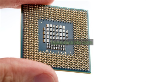
A System-in-Package (시피) substrate is a type of electronic substrate used to integrate multiple components into a single package, creating a compact and efficient system. SiP substrates serve as the foundation for assembling various semiconductor devices, such as integrated circuits (IC (영어)), passive components, and other electronic elements, into a unified module. This integration enhances functionality while reducing the overall size and complexity of electronic systems.
SiP substrates typically consist of several layers, including a base layer for mechanical support, intermediate layers for electrical interconnections, and top layers for mounting components. The substrate’s design allows for high-density interconnects, which facilitate the integration of different technologies within a single package. This integration can include a mix of digital, analog, 무선 주파수 (RF), and power components, making SiP a versatile solution for complex electronic applications.
One of the primary advantages of SiP substrates is their ability to reduce the footprint and weight of electronic devices. By consolidating multiple components into a single package, SiP technology can lead to smaller, 라이터, and more efficient devices. 또한, SiP substrates can improve performance by minimizing signal delay and interference through optimized interconnect routing and reduced trace lengths.
SiP technology is widely used in various applications, 스마트폰 포함, 웨어러블, 자동차 전자 장치, 및 의료 기기. It enables the creation of compact, high-performance systems that meet the demands of modern electronic applications, making it a critical technology in the advancement of electronic devices and systems.

SIP 기판 제조업체
무엇입니까 SIP Substrate 디자인 지침?
시스템 인 패키지 (시피) 기판 design guidelines are essential for ensuring that SiP assemblies meet performance, 신뢰도, and manufacturability requirements. These guidelines encompass several key aspects:
- Layer Design: Design the substrate with multiple layers to accommodate different components and interconnects. Ensure that the layer stack-up provides adequate mechanical support and electrical performance. 일반적 으로, this involves a base layer for structural integrity, intermediate layers for signal routing, and top layers for component mounting.
- Interconnects: Optimize the design of interconnects to minimize signal delay and interference. Use high-density interconnects to accommodate various components and ensure reliable signal transmission. Consider the use of fine-pitch pads and vias for effective electrical connections.
- 열 관리: Incorporate thermal management strategies to dissipate heat generated by the components. Use heat sinks, 열 바이어스, and appropriate material selections to maintain thermal performance and prevent overheating of sensitive components.
- Electrical Performance: Design the substrate to meet the electrical performance requirements of the integrated components. This includes impedance control, 신호 무결성, and power distribution. Implement proper grounding and shielding techniques to reduce noise and crosstalk.
- 기계적 고려 사항:Ensure the substrate design supports mechanical stability and durability. This involves selecting appropriate materials and designing for thermal expansion and contraction to avoid mechanical stress on the components.
- 제조 가능성: Design the substrate with manufacturability in mind. This includes considering the capabilities of fabrication processes, ease of assembly, and the potential for defects. Use design for manufacturability (디에프엠) principles to optimize the substrate for reliable production.
- 테스트 및 검증: Include provisions for testing and validation of the SiP substrate. This ensures that the final product meets all performance and reliability standards before it is deployed in end-use applications.
이러한 디자인 지침을 준수함으로써, engineers can create SiP substrates that deliver high performance, 신뢰도, and efficiency, 광범위한 고급 전자 응용 분야에 적합합니다..
의 장점 SIP Substrate
시스템 인 패키지 (시피) 기판 offer several advantages that make them highly desirable for modern electronic applications. 주요 이점은 다음과 같습니다:
- Compact Size: SiP substrates enable the integration of multiple components into a single package, significantly reducing the overall size and weight of electronic devices. This compactness is essential for portable and space-constrained applications, 스마트 폰과 같은, 웨어러블, 및 IoT 장치.
- Improved Performance: By consolidating components into a single package, SiP substrates can reduce signal delay and interference. The optimized routing of interconnects and minimized trace lengths enhance the overall performance and speed of electronic systems.
- 비용 효율성: Although the initial design and development of SiP substrates can be complex, they often lead to cost savings in the long run. The reduction in the number of discrete components and the simplified assembly process can lower manufacturing costs and reduce the total bill of materials.
- 향상된 신뢰성: SiP substrates can improve the reliability of electronic systems by minimizing the number of connections between components. Fewer connections reduce the risk of mechanical failure and solder joint issues, leading to increased durability and longevity of the final product.
- 설계의 유연성: SiP technology allows for the integration of diverse components, such as digital, analog, 무선 주파수 (RF), and power devices, within a single package. This flexibility supports the creation of multifunctional systems tailored to specific application needs.
- Reduced Power Consumption: The compact design of SiP substrates can contribute to lower power consumption by shortening the distances between components and optimizing power distribution. This efficiency is crucial for battery-operated devices and energy-sensitive applications.
- Faster Time-to-Market: Integrating multiple components into a single SiP substrate can streamline the development process and reduce time-to-market. This accelerated timeline can be a competitive advantage in rapidly evolving technology sectors.
- 향상된 열 관리: Advanced SiP substrates can include thermal management features such as heat sinks and thermal vias, which help dissipate heat more effectively. This management is critical for maintaining the performance and reliability of high-power components.
전반적, SiP substrates offer a range of advantages that enhance the performance, 신뢰도, and efficiency of electronic devices, making them a valuable technology in the advancement of modern electronics.
무엇입니까 SIP Substrate 제작 과정?
The fabrication process for System-in-Package (시피) substrates involves several intricate steps to create a high-density, multi-component package. Here’s an overview of the typical SiP substrate fabrication process:
- 디자인 및 레이아웃: The process begins with designing the SiP substrate layout. This includes defining the layer stack-up, interconnect patterns, and component placements. Advanced design tools are used to optimize the layout for electrical performance, 열 관리, 및 제조 가능성.
- 재료 선택: Choose appropriate materials for the substrate layers based on electrical, 열, and mechanical requirements. Common materials include epoxy resins, glass fibers for FR4, and specialized high-performance materials for advanced applications.
- Layer Fabrication: 기판은 여러 층으로 구성되어 있습니다. Each layer is fabricated separately and may include copper foils, 유전체 재료, and other components. These layers are patterned using photolithography, 에칭, and plating processes to create the necessary circuitry and interconnects.
- Layer Alignment and Bonding: Once individual layers are fabricated, they are aligned and bonded together. This is typically done using a process called lamination, where layers are stacked and fused together under heat and pressure. Accurate alignment is crucial to ensure proper electrical connections and mechanical stability.
- Via and Hole Drilling: 비아 (vertical interconnects) and holes are drilled into the substrate to connect different layers and accommodate component leads. This process involves precise drilling techniques to create the required openings without damaging the substrate.
- Plating and Metallization: After drilling, vias and holes are plated with metal to form electrical connections between layers. This process typically involves electroplating or electroless plating to deposit a thin layer of metal, such as copper, onto the inner walls of the vias.
- Component Integration: Components such as ICs, passive devices, and other electronic elements are mounted onto the substrate. This step involves precise placement and soldering of components, often using automated pick-and-place machines and reflow soldering techniques.
- Encapsulation and Protection: The assembled SiP substrate may be encapsulated or coated with protective materials to safeguard against environmental factors such as moisture, dust, 및 기계적 스트레스. This step helps enhance the durability and reliability of the final product.
- 테스트 및 검사:Rigorous testing and inspection are conducted to ensure the SiP substrate meets all performance and reliability criteria. 여기에는 전기 테스트가 포함됩니다, 열 분석, and mechanical inspections to verify that the substrate functions as intended and meets quality standards.
- Final Packaging:Once testing is complete, the SiP substrate is prepared for final packaging. This may involve cutting the substrate into individual units, applying protective coatings, and preparing the package for shipment or integration into end-use products.
The SiP substrate fabrication process combines advanced materials, 정밀한 제조 기술, and rigorous quality control to produce high-performance, reliable electronic systems.
세라믹의 적용 SIP Substrate
Ceramic System-in-Package (시피) substrates are used in a variety of high-performance applications due to their superior electrical, 열, 및 기계적 성질. Here are some key applications of ceramic SiP substrates:
- 통신:Ceramic SiP substrates are widely used in telecommunications equipment, 베이스 스테이션 포함, routers, and network infrastructure. Their excellent high-frequency performance and thermal stability are essential for handling the high-speed and high-power signals in these systems.
- 자동차 전장: 자동차 산업에서, ceramic SiP substrates are employed in advanced driver-assistance systems (ADAS (장애인)), 엔진 제어 장치 (ECU (영문)), 및 인포테인먼트 시스템. Their durability and ability to withstand high temperatures and vibrations make them suitable for automotive environments.
- 의료 기기: Medical devices, such as imaging equipment, diagnostic instruments, 및 이식 가능한 장치, benefit from ceramic SiP substrates due to their biocompatibility, 신뢰도, and precise performance. The thermal management capabilities of ceramics also help maintain the stability of sensitive medical electronics.
- 항공우주 및 방위 산업:Ceramic SiP substrates are used in aerospace and defense applications, including satellite systems, 레이다, 및 통신 시스템. Their high thermal conductivity, reliability in extreme conditions, and resistance to radiation make them ideal for critical applications in these sectors.
- 소비자 가전제품: High-performance consumer electronics, 스마트 폰과 같은, 정제, 그리고 웨어러블, often utilize ceramic SiP substrates for their compact size, 우수한 열 관리, and ability to handle high-frequency signals. This enables the integration of multiple components into a small package while maintaining performance.
- 파워 일렉트로닉스: 전력 전자 제품에서, ceramic SiP substrates are used for power management and conversion systems, including DC-DC converters and power amplifiers. The ceramics’ ability to dissipate heat effectively and handle high power levels is crucial for efficient power regulation.
- Industrial Automation: Ceramic SiP substrates are found in industrial automation equipment, such as robotics, 제어 시스템, and sensors. Their robustness and ability to operate in harsh environments ensure reliable performance in industrial settings.
전반적, ceramic SiP substrates offer a range of benefits, 높은 열전도율을 포함하여, 전기적 성능, 및 기계적인 안정성, making them suitable for demanding applications across various industries.
에 대한 FAQ SIP Substrate
What are the advantages of using SiP substrates?
SiP substrates offer advantages like reduced size and weight of electronic devices, improved performance with reduced signal delay, cost efficiency through fewer discrete components, and enhanced reliability due to fewer connections.
What materials are commonly used for SiP substrates?
Common materials for SiP substrates include epoxy resins, ceramic materials, and high-performance composites. The choice of material depends on the specific requirements of the application, such as thermal management and electrical performance.
How does SiP differ from traditional PCB (Printed Circuit Board) technology?
Unlike traditional PCBs, which typically support a single layer of circuitry, SiP substrates integrate multiple components and layers into a single package. This allows for more compact designs and higher functionality in a smaller footprint.
What are the typical applications of SiP substrates?
SiP substrates are used in various applications, 통신 포함, 자동차 전자 장치, 의료 기기, 소비자 가전제품, 항공 우주, 및 전력 전자 장치. They are valued for their ability to consolidate multiple functions into a single package.
What are the challenges in designing SiP substrates?
Challenges include managing thermal dissipation, ensuring precise alignment of components, optimizing signal integrity, and addressing manufacturing complexities. Proper design and fabrication processes are crucial to overcoming these challenges.
How is the quality of SiP substrates ensured?
Quality is ensured through rigorous testing and inspection processes, including electrical performance testing, 열 분석, and mechanical inspections. Adhering to design guidelines and using reliable manufacturing techniques also contribute to high-quality outcomes.


) 세라믹 기판 제조업체")
