
Single-Layer Ceramic Substrate 생산자
단층 세라믹 기판 제조업체,Single-layer ceramic substrates are thin, flat plates composed of materials like alumina or aluminum nitride. They serve as essential bases for mounting electronic components in circuits, providing high thermal conductivity, 우수한 전기 절연성, 및 기계적 강도. These substrates are pivotal in industries ranging from telecommunications and automotive electronics to aerospace and medical devices, where reliability, 방열, and dimensional stability are critical. Their versatility supports high-frequency applications and ensures operational efficiency in harsh environments, making them indispensable in modern electronics for optimizing performance and reliability.
무엇입니까 Single-Layer Ceramic Substrate?
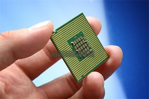
A single-layer ceramic substrate, commonly used in electronics and microelectronics, refers to a flat, thin plate made from ceramic materials like alumina (알2O3) 또는 질화알루미늄 (알엔(AlN)). These substrates serve as a foundation for mounting electronic components such as integrated circuits (IC (영어)), 저항기, 커패시터, and other devices in electronic circuits. The ceramic material offers several advantages, including excellent thermal conductivity, 기계적 강도, and electrical insulation properties.
The manufacturing process typically involves forming the ceramic material into a thin, flat sheet, which is then fired at high temperatures to achieve the desired properties. Afterward, conductive pathways or pads are applied using techniques like screen printing or thin-film deposition, which allows for electrical connections between components. These substrates are crucial in miniaturizing electronic devices, improving thermal management, and ensuring reliability in harsh operating conditions.
Applications of single-layer ceramic substrates span various industries, 통신 포함, 항공 우주, 자동차 전자 장치, 및 소비자 전자 제품. They are particularly valued in applications requiring high-frequency operation, high power density, or where thermal management is critical. The single-layer configuration simplifies the manufacturing process compared to multi-layer substrates, making them cost-effective for certain applications while still offering robust performance in demanding environments.

단층 세라믹 기판 제조업체
무엇입니까 Single-Layer Ceramic Substrate 디자인 지침?
에 대한 디자인 지침 single-layer ceramic substrates are crucial to ensure the reliability, 공연, 전자 회로의 제조 가능성. 다음은 몇 가지 주요 지침입니다:
- 재료 선택: 알루미나와 같은 세라믹 재료를 선택하십시오 (알2O3) 또는 질화알루미늄 (알엔(AlN)) based on the specific requirements of the application, including thermal conductivity, 유전 상수, 및 기계적 강도.
- Thickness: The thickness of the ceramic substrate affects its mechanical strength and thermal performance. 일반적 으로, substrates range from tens to hundreds of micrometers thick, depending on the application’s thermal and mechanical requirements.
- Layout and Placement: Arrange components on the substrate to minimize signal path lengths, reduce parasitic capacitance and inductance, and optimize thermal dissipation. Place high-power components where heat dissipation is efficient.
- 비아 디자인: Vias are used to connect conductive layers on the substrate. Design vias carefully to minimize signal distortion and ensure reliable electrical connections. Consider via size, 음조, and placement for optimal electrical performance.
- Conductor Width and Spacing: Define conductor widths and spacing based on the current-carrying capacity, signal integrity requirements, and manufacturing capabilities. Ensure adequate spacing to prevent electrical breakdown and crosstalk.
- Dielectric Layers: If using multi-layer ceramics or integrated passive components (IPC), specify dielectric layer properties to achieve desired capacitance, inductance, and impedance characteristics.
- 열 관리: Incorporate features such as thermal vias, 방열판, or metalized pads to enhance heat dissipation and prevent overheating of components.
- 제조 가능성: Design for manufacturability by considering substrate size, panelization, tolerances, and alignment features for automated assembly processes like screen printing, laser trimming, and soldering.
- 환경 고려 사항: Account for environmental factors such as temperature extremes, 습도, and mechanical stress to ensure substrate reliability over the intended operational lifetime.
- 테스트 및 검증: Plan for testing and validation procedures to ensure that the designed substrate meets performance specifications and reliability requirements under operational conditions.
Following these guidelines helps ensure that the single-layer ceramic substrate performs optimally in its intended application, meets reliability standards, and facilitates efficient manufacturing processes.
의 장점 Single-Layer Ceramic Substrate
Single-layer ceramic substrates offer several advantages that make them ideal for various electronic applications:
- 열 관리: Ceramic materials like alumina (알2O3) 및 질화 알루미늄 (알엔(AlN)) have excellent thermal conductivity. This property allows single-layer ceramic substrates to efficiently dissipate heat generated by electronic components, improving overall reliability and longevity.
- 전기 절연: Ceramic substrates provide high electrical insulation, which is essential for preventing electrical leakage and ensuring proper signal integrity in electronic circuits. This insulation capability also reduces the risk of short circuits.
- 기계적 강도:Ceramic materials exhibit high mechanical strength and stiffness relative to their weight. This characteristic makes single-layer ceramic substrates durable and resistant to mechanical stresses such as bending or vibration, enhancing the reliability of electronic assemblies.
- 치수 안정성: Ceramic substrates maintain their shape and dimensions over a wide range of operating temperatures, from sub-zero to high temperatures, without significant expansion or contraction. This stability ensures consistent performance of electronic components in varying environmental conditions.
- 소형화: Single-layer ceramic substrates can be manufactured with very thin profiles while maintaining structural integrity and electrical performance. This capability supports the miniaturization of electronic devices and enables the integration of complex circuits in a compact space.
- Compatibility with High Frequencies: Due to their low dielectric losses and stable electrical properties over a wide frequency range, ceramic substrates are suitable for applications involving high-frequency signals. They minimize signal loss and distortion, making them ideal for telecommunications, RF/microwave circuits, and high-speed data transmission.
- 내화학성: Ceramic materials are typically resistant to chemicals, 습기, and corrosive environments. This property enhances the substrate’s reliability in harsh operating conditions, such as automotive electronics, aerospace applications, and industrial environments.
- Cost-Effective Manufacturing: Compared to multi-layer ceramic substrates, single-layer designs are simpler to manufacture, involving fewer processing steps such as fewer layers to print, fire, and align. This simplicity often translates to lower manufacturing costs for certain applications.
전반적, single-layer ceramic substrates offer a combination of thermal, 전기의, 기계적인, and chemical properties that make them highly advantageous for a wide range of electronic and microelectronic applications, particularly where reliability, 공연, and compact design are critical considerations.
무엇입니까 Single-Layer Ceramic Substrate 제작 과정?
The fabrication process of a single-layer ceramic substrate typically involves several key steps to produce a flat, thin plate that serves as a foundation for mounting electronic components. Here is a generalized outline of the fabrication process:
- 재료 선택: Choose ceramic materials based on the application requirements. 일반적인 재료에는 알루미나가 포함됩니다. (알2O3) 및 질화 알루미늄 (알엔(AlN)), selected for their thermal conductivity, 전기 절연 특성, 및 기계적 강도.
- Formulation and Preparation: Ceramic powders are mixed with binders and solvents to form a slurry. This slurry is then cast or tape-cast into a green sheet with the desired thickness. The green sheet consists of the ceramic material in a pliable, unfired state.
- Green Sheet Processing: The green sheets undergo processes such as drying to remove solvents and binders, and then are cut into individual substrate blanks of the desired size and shape.
- Screen Printing: Conductive materials such as silver, 금, or copper pastes are screen printed onto the green substrate blanks to create the circuit patterns, 패드, and vias. These conductive elements are essential for establishing electrical connections between components.
- Drying and Firing: After printing, the substrate blanks undergo a controlled drying process to remove any remaining solvents. Subsequently, the fired in a kiln at high temperatures (typically around 1000°C to 1700°C depending on the ceramic material) to sinter the ceramic particles and fuse the conductive materials, forming a dense, solid substrate.
- Post-Firing Processing: Once fired, the substrates may undergo additional processes such as laser trimming to adjust resistor values or metallization of contact pads to improve solderability.
- 표면 마무리: The substrates may undergo surface treatments such as polishing or coating to achieve specific surface smoothness or to enhance specific properties like adhesion or moisture resistance.
- 품질 관리 및 테스트: 제작 공정 전반에 걸쳐, quality control measures ensure that substrates meet dimensional tolerances, electrical specifications, and reliability standards. Testing may include electrical continuity checks, dielectric strength tests, and thermal cycling tests to verify performance under various conditions.
- Packaging and Delivery: 마침내, substrates are inspected, packaged to protect them during shipping, and delivered to customers or further integrated into electronic assemblies.
This process outline can vary depending on specific requirements, material choices, and manufacturing capabilities of different suppliers. Each step is critical to ensuring the final substrate meets the stringent performance and reliability standards demanded by modern electronic applications.
세라믹의 적용 Single-Layer Ceramic Substrate
Single-layer ceramic substrates find wide application across various industries and technologies due to their excellent thermal, 전기의, 및 기계적 성질. 다음은 몇 가지 주요 응용 프로그램입니다:
- Electronics and Microelectronics: Single-layer ceramic substrates serve as essential components in electronic circuits, providing a stable and reliable platform for mounting integrated circuits (IC (영어)), 저항기, 커패시터, and other components. They are used in consumer electronics, telecommunications equipment, computer peripherals, and control systems.
- High-Frequency Applications: Due to their low dielectric losses and stable electrical properties over a wide frequency range, ceramic substrates are ideal for high-frequency applications. They are used in RF/microwave circuits, 레이더 시스템, wireless communication devices, and satellite communications equipment.
- 파워 일렉트로닉스: 전력 전자 제품에서, ceramic substrates are employed for their excellent thermal conductivity and electrical insulation properties. 그들은 전력 모듈에 사용됩니다, 모터 드라이브, 인버터, and converters where efficient heat dissipation and electrical isolation are critical.
- 자동차 전장: Ceramic substrates are utilized in automotive applications where reliability, temperature stability, and resistance to vibrations and harsh environments are essential. They are used in engine control units (ECU (영문)), 센서, LED 조명 시스템, and power electronics in electric and hybrid vehicles.
- 항공우주 및 방위 산업: In aerospace and defense industries, ceramic substrates are valued for their high reliability, 열 관리 기능, and ability to withstand extreme temperatures and environmental conditions. They are used in avionics, 레이더 시스템, 통신 장비, missile guidance systems, and satellite payloads.
- 의료 기기: Ceramic substrates are used in medical devices and equipment where biocompatibility, 신뢰도, and resistance to sterilization processes are required. They are used in implantable devices, 진단 장비, medical imaging systems, and laboratory instrumentation.
- Industrial Applications:Ceramic substrates find application in industrial automation, process control systems, 로봇공학, and power distribution equipment. Their robustness, 열 관리 기능, and resistance to chemicals make them suitable for harsh industrial environments.
- LED and Optoelectronics: Ceramic substrates are used in LED (Light Emitting Diode) packaging and optoelectronic devices where thermal management is crucial to maintain LED efficiency and longevity. They provide a stable platform for mounting LEDs and other optical components.
전반적, the versatility and performance characteristics of single-layer ceramic substrates make them indispensable in a wide range of advanced technology applications, contributing to the efficiency, 신뢰도, and miniaturization of electronic systems across various industries.
자주 묻는 질문(FAQ 약 Single-Layer Ceramic Substrate
What is a single-layer ceramic substrate?
A single-layer ceramic substrate is a thin, flat plate made from ceramic materials such as alumina (알2O3) 또는 질화알루미늄 (알엔(AlN)). It serves as a base for mounting electronic components in circuits, providing thermal management, 전기 절연, 및 기계적 지원.
What are the advantages of using single-layer ceramic substrates?
Single-layer ceramic substrates offer advantages such as excellent thermal conductivity, high electrical insulation, 기계적 강도, dimensional stability over a wide temperature range, and compatibility with high-frequency applications. They are also cost-effective compared to multi-layer substrates in certain applications.
What industries use single-layer ceramic substrates?
Single-layer ceramic substrates are used in various industries including electronics (for ICs, 저항기, 커패시터), 통신, 자동차 전자 장치, 항공 우주, 파워 일렉트로닉스, 의료 기기, LED/optoelectronics, and industrial automation.
What are the thermal management capabilities of single-layer ceramic substrates?
Ceramic substrates have excellent thermal conductivity, allowing them to efficiently dissipate heat generated by electronic components. This property helps in maintaining component reliability and longevity, especially in high-power and high-temperature applications.
What considerations should be made when designing with single-layer ceramic substrates?
Design considerations include material selection based on thermal and electrical properties, layout optimization for signal integrity and heat dissipation, via design for electrical connectivity, and ensuring compatibility with manufacturing processes for cost-effective production.
What testing and quality control measures are used for single-layer ceramic substrates?
Testing may include checks for dimensional accuracy, 전기적 연속성, 절연 내력, 열 사이클링, and reliability under various environmental conditions. Quality control ensures that substrates meet performance specifications and reliability standards.
What are the environmental and chemical resistance properties of single-layer ceramic substrates?
Ceramic substrates are generally resistant to chemicals, 습기, and corrosion, making them suitable for harsh environments encountered in automotive, 항공 우주, 및 산업 응용 분야. They also exhibit good stability in the presence of temperature extremes.
 기판 제조업체")
 세라믹 기판 제조업체")
 세라믹 기판 제조업체")
) 세라믹 기판 제조업체")
 세라믹 기판 제조업체")


