
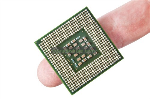
Other High Speed Materials Substrate 생산자
다른 고속 재료 기판 제조 업체,Other high-speed materials substrates are advanced laminates tailored for high-frequency and high-speed electronic applications. These substrates often feature low dielectric constants and low loss tangents, which enhance signal integrity and reduce signal degradation in RF and microwave circuits. Many of these materials are engineered for exceptional thermal stability and low moisture absorption, ensuring reliability in demanding environments. With capabilities for fine-line processing, they support intricate multilayer designs and high-density interconnects. Commonly utilized in telecommunications, 항공 우주, and automotive sectors, these high-speed substrates provide engineers with versatile solutions for cutting-edge electronic systems that require optimal performance.
What is Other High Speed Materials Substrate?
Other High Speed Materials Substrate refers to substrates used for high-frequency and high-speed signal transmission in electronic components. These substrate materials typically feature low dielectric constants and low loss characteristics, effectively reducing signal attenuation and delay, thereby enhancing the performance of electronic devices.
In high-frequency applications, the dielectric properties of materials are crucial. Common high-speed materials include polytetrafluoroethylene (폴리에틸렌), fluoropolymer, and various advanced ceramics and composite materials. These materials are widely used in microwave communication, 레이더 시스템, and high-speed digital circuits.
The design of high-speed material substrates considers several factors, including the number of layers, dielectric layers between layers, and the thickness of copper foil. These parameters directly affect signal integrity and circuit thermal management. 또한, the manufacturing process of high-speed material substrates is critical, requiring uniformity and stability of the materials to avoid unnecessary losses at high frequencies.
With the development of 5G communication and the Internet of Things, the demand for high-speed material substrates continues to grow, driving the research and application of new materials. In the future, these substrates are expected to play a key role in more advanced electronic products, improving overall device performance and reliability.

다른 고속 재료 기판 제조 업체
What is the Other High Speed Materials Substrate Design Guidelines?
The design guidelines for Other High Speed Materials Substrate focus on optimizing performance in high-frequency applications. Here are key considerations:
- 재료 선택: Choose materials with low dielectric constants and low loss tangents. 일반적인 재료에는 PTFE가 포함됩니다., fluoropolymers, and advanced ceramics.
- 레이어 구조: Design multi-layer structures to minimize signal path length and reduce parasitic capacitance. Ensure optimal layer stack-up to balance electrical performance and mechanical stability.
- 트레이스 폭 및 간격: Use appropriate trace widths and spacing to manage impedance and minimize signal loss. Consider controlled impedance design for differential pairs and single-ended signals.
- Ground Planes: Implement solid ground planes to enhance signal integrity and provide shielding against electromagnetic interference (EMI (이엠아이)). This helps reduce crosstalk between traces.
- 열 관리: Ensure proper thermal management to dissipate heat generated by high-speed components. Consider thermal vias and heat sinks where necessary.
- 비아 디자인: Use blind or buried vias to minimize signal path length and maintain high-frequency performance. Pay attention to via plating and back-drilling to reduce reflections.
- 시뮬레이션 및 테스트: Utilize simulation tools to model signal integrity, 전자기 간섭, and thermal performance. Conduct rigorous testing to validate design against specifications.
- Manufacturing Considerations: Collaborate with manufacturers early in the design process to ensure the feasibility of the substrate design, especially for intricate geometries and materials.
이 지침을 준수함으로써, designers can enhance the performance and reliability of high-speed materials substrates in various applications, 통신 포함, 레이더 시스템, and high-speed digital circuits.
The advantages of Other High Speed Materials Substrate
High-speed materials substrates offer several advantages, particularly in applications requiring high-frequency performance and superior electrical characteristics. Here are some of the key advantages:
- High-Frequency Performance: High-speed materials, such as PTFE (폴리테트라플루오로에틸렌), 구체의, and certain advanced ceramics, provide excellent performance at high frequencies. This makes them ideal for RF (무선 주파수) 그리고 마이크로파 응용(microwave applications).
- Low Dielectric Constant (디케이): These materials typically have a low dielectric constant, which helps minimize signal loss and propagation delay, ensuring faster signal transmission.
- 낮은 유전 손실 (디에프): High-speed materials exhibit low dielectric loss, reducing energy dissipation and maintaining signal integrity over long distances and at high frequencies.
- 열 안정성: Many high-speed substrates, such as Rogers and other advanced laminates, offer excellent thermal stability, maintaining their properties across a wide temperature range. This is crucial for applications in harsh environments.
- 높은 열전도율:Some high-speed materials, especially certain ceramics and metal composites, have high thermal conductivity, allowing efficient heat dissipation. This is essential for high-power applications to prevent overheating.
- 치수 안정성: These materials exhibit good dimensional stability, which means they maintain their size and shape under various environmental conditions, including humidity and temperature changes. This ensures consistent performance and reliability.
- 내화학성: High-speed substrates often have good resistance to chemicals and environmental factors, enhancing their durability and lifespan in challenging conditions.
- 기계적 강도: Advanced high-speed materials can offer superior mechanical strength and rigidity, supporting the integrity of the substrate during manufacturing, handling, and operation.
- Compatibility with Advanced Manufacturing Processes: These materials are often compatible with advanced manufacturing processes, such as fine-line etching and high-density interconnect (HDI는) technology, allowing for the creation of complex and miniaturized designs.
- Enhanced Signal Integrity: The combination of low dielectric constant and low loss tangent helps in maintaining high signal integrity, reducing issues like signal attenuation and cross-talk, which are critical in high-speed digital and RF circuits.
- 전자기 간섭 감소 (EMI (이엠아이)): High-speed materials can help in reducing EMI, providing better performance in environments with high levels of electromagnetic interference.
By leveraging these advantages, high-speed material substrates enable the development of advanced electronic systems with superior performance, 신뢰도, and efficiency, particularly in applications like telecommunications, 항공 우주, 방어, and high-speed computing.
What is the Other High Speed Materials Substrate Fabrication Process?
The fabrication process for high-speed materials substrates involves several key steps, each designed to ensure the precise manufacturing and high performance of the substrate. 다음은 일반적인 프로세스에 대한 개요입니다:
- 재료 선택: Choose appropriate high-speed materials, such as PTFE, 구체의, or advanced ceramics, based on the specific application requirements. Consider factors like dielectric constant, 열전도율, 및 기계적 강도.
- Laminating: Combine the chosen high-speed material with copper foil to create the laminate. This involves bonding the copper foil to the dielectric material using heat and pressure. The process ensures strong adhesion and the formation of a uniform laminate.
- 드릴링: Drill holes (비아) in the laminate to create pathways for electrical connections between different layers of the substrate. Advanced laser drilling or mechanical drilling techniques are used to achieve high precision and accuracy, especially for high-density designs.
- Desmearing and Hole Preparation: Clean the drilled holes to remove any debris and smear caused by the drilling process. This step is crucial for ensuring reliable electrical connections. Chemical processes or plasma etching are often used for desmearing.
- Electroless Copper Deposition: Deposit a thin layer of copper inside the drilled holes using an electroless plating process. This provides a conductive base for subsequent electroplating and ensures reliable electrical connectivity between layers.
- Imaging and Etching: Apply a photoresist to the copper-clad laminate and use photolithography to define the circuit patterns. Expose the photoresist to UV light through a mask, then develop the photoresist to reveal the desired circuit patterns. Etch away the exposed copper to create the circuit traces.
- 도금: Electroplate additional copper onto the circuit traces and inside the vias to increase the thickness and improve the conductivity of the connections. This step ensures robust electrical performance, especially for high-current applications.
- 솔더 마스크 적용: Apply a solder mask over the substrate to protect the circuit traces and prevent short circuits during soldering. The solder mask also helps to reduce corrosion and provides insulation between conductive paths.
- 표면 마감: Apply a surface finish, such as ENIG (무전해 니켈 침지 금), HASL (열풍 솔더 레벨링), 또는 OSP (유기 납땜성 방부제), to the exposed copper areas. The surface finish enhances solderability and protects the copper from oxidation.
- 검사 및 테스트: Perform thorough inspection and testing of the fabricated substrate to ensure it meets the required specifications. 여기에는 육안 검사가 포함됩니다, 전기 테스트, and reliability testing to verify the performance and quality of the substrate.
- 최종 조립: If the substrate is part of a multilayer PCB, additional layers are laminated, drilled, and processed as needed. The layers are aligned and bonded together to create the final multilayer structure.
- 포장 및 배송: Once the substrate passes all quality checks, it is cleaned, packaged, and prepared for shipping. Proper packaging ensures the substrate remains free from damage and contamination during transportation.
다음 단계를 따릅니다, manufacturers can produce high-speed material substrates that offer superior performance, 신뢰도, and efficiency for advanced electronic applications.
The application of ceramic Other High Speed Materials Substrate
Ceramic high-speed materials substrates are used in a wide range of applications due to their excellent electrical, 열, 및 기계적 성질. Here are the primary applications:
- High-Frequency Communication Systems: Ceramic substrates are ideal for RF and microwave communication systems, including satellite communications, 레이더 시스템, and wireless base stations. Their low dielectric constant and low loss tangent ensure minimal signal loss and high signal integrity.
- 파워 일렉트로닉스: 전력 전자 제품에서, ceramic substrates are used in devices like power transistors, 인버터, and converters. Their high thermal conductivity helps efficiently dissipate heat, enhancing the performance and reliability of these devices.
- 자동차 전장: Ceramic substrates are widely used in automotive applications, including engine control units (ECU (영문)), 센서, and power modules for electric and hybrid vehicles. Their thermal stability and durability make them suitable for harsh automotive environments.
- 항공우주 및 방위 산업: Ceramic substrates are employed in aerospace and defense applications such as avionics, missile guidance systems, and electronic warfare equipment. Their ability to withstand extreme temperatures and high radiation levels is crucial in these environments.
- 의료 기기: High-speed ceramic substrates are used in medical devices like imaging systems, 진단 장비, 및 이식 가능한 장치. Their biocompatibility and reliability ensure safe and effective performance in medical applications.
- 통신: Ceramic substrates are used in telecommunication infrastructure, 베이스 스테이션 포함, 리피터, and antennas. Their high-frequency performance and stability support the growing demand for faster and more reliable communication networks.
- 소비자 가전제품: In consumer electronics, ceramic substrates are found in high-performance devices such as smartphones, 정제, 그리고 웨어러블. 컴팩트한 크기, 높은 신뢰성, and superior thermal management support the miniaturization and advanced functionality of these devices.
- LED 조명: Ceramic substrates are used in high-power LED lighting systems due to their excellent thermal management properties. They help maintain the performance and longevity of LEDs by efficiently dissipating heat generated during operation.
- Industrial Automation: Ceramic substrates are employed in industrial automation systems, including robotics, 센서, and control units. Their robustness and reliability ensure consistent performance in demanding industrial environments.
- Semiconductor Testing: Ceramic substrates are used in probe cards and test sockets for semiconductor testing. Their precision, 내구성, and electrical performance make them suitable for testing high-speed and high-frequency semiconductor devices.
- Renewable Energy: In renewable energy systems, such as solar inverters and wind turbine control units, ceramic substrates provide reliable performance and efficient thermal management, contributing to the overall efficiency and durability of these systems.
By leveraging the unique properties of ceramic high-speed materials substrates, these applications achieve enhanced performance, 신뢰도, and efficiency, supporting the development of advanced technologies across various industries.
FAQs about Other High Speed Materials Substrate
What are high-speed materials substrates?
High-speed materials substrates are specialized materials used in electronic circuits to handle high-frequency signals with minimal loss and interference. They are designed to maintain signal integrity and performance in high-speed and high-frequency applications.
What materials are commonly used for high-speed substrates?
일반적인 재료에는 PTFE가 포함됩니다. (폴리테트라플루오로에틸렌), 구체의, and advanced ceramics like alumina and beryllium oxide. These materials offer low dielectric constants, low loss tangents, and excellent thermal stability.
Why are high-speed materials important in electronics?
They are crucial for applications that require fast data transmission and high-frequency performance, such as telecommunications, 항공 우주, and high-speed computing. They help in reducing signal loss, maintaining signal integrity, and managing heat.
How do high-speed substrates differ from standard PCB substrates?
High-speed substrates typically have lower dielectric constants and loss tangents compared to standard PCB substrates, like FR4. This makes them better suited for high-frequency applications, 신호 무결성과 최소 손실이 중요한 경우.
What is the typical fabrication process for high-speed substrates?
The process generally includes material selection, laminating, 드릴링, desmearing, electroless copper deposition, imaging, 에칭, 도금, 솔더 마스크 적용, 표면 마감, and final inspection.
What are the advantages of using ceramic high-speed substrates?
Ceramic substrates offer high thermal conductivity, 우수한 전기적 성능, 및 기계적 강도. They are ideal for high-power and high-frequency applications, providing reliable performance in extreme conditions.


) 세라믹 기판 제조업체")
