
Mitsubishi BGA Substrate 생산자
미쓰비시 BGA 기판 제조업체,Mitsubishi BGA Substrate is a cutting-edge solution for high-density semiconductor packaging. Known for its advanced design and manufacturing, it offers excellent thermal management and electrical performance crucial for modern electronic devices. Mitsubishi BGA Substrate supports complex integrated circuits with high pin counts, ensuring reliable connectivity and signal integrity. Its materials provide low thermal expansion and exceptional mechanical strength, making it suitable for applications in telecommunications, 컴퓨팅, and automotive electronics. Engineers rely on Mitsubishi BGA Substrate for its precision, 내구성, and ability to meet stringent requirements of advanced packaging technologies, facilitating compact and efficient electronic systems.
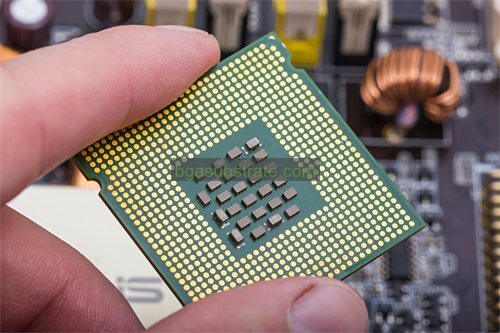
What is Mitsubishi BGA Substrate?
Mitsubishi BGA Substrate refers to Ball Grid Array (BGA (영어)) substrates manufactured by Mitsubishi Electric Corporation. These substrates are crucial components in electronic packaging, facilitating the interconnection between integrated circuits (IC (영어)) and PCBs. Mitsubishi’s BGA substrates are known for their high reliability, thermal performance, and electrical integrity, making them suitable for various applications requiring compact and efficient circuit integration.
These substrates typically feature advanced materials and precise manufacturing processes to ensure optimal performance in demanding environments. They are designed to support high-density interconnects, allowing for the integration of multiple ICs in a compact space while maintaining signal integrity and thermal management.
Mitsubishi’s expertise in BGA substrates extends to various forms, including those optimized for different thermal management needs, 고주파 응용 분야, and specific mechanical requirements. Their products often adhere to industry standards and are tailored to meet the evolving needs of modern electronics, ensuring robust performance and reliability in electronic assemblies.

미쓰비시 BGA 기판 제조업체
What is the Mitsubishi BGA Substrate Design Guidelines?
The design guidelines for Mitsubishi BGA substrates provide detailed instructions and recommendations for engineers and designers to ensure the optimal performance, 신뢰도, and manufacturability of their BGA-based electronic assemblies. These guidelines typically cover several key aspects:
- 패드 및 비아 디자인: Specifications for pad sizes, shapes, and pitches are detailed to ensure proper soldering and electrical connectivity. Guidelines for via sizes, placement, and anti-pad requirements are also included to minimize signal interference and ensure thermal management.
- 레이어 스택업: Recommendations for the layer configuration and materials used in the substrate construction to achieve desired electrical properties, thermal performance, 및 기계적인 안정성. This includes considerations for signal integrity, power distribution, and grounding strategies.
- 열 관리: Guidelines for thermal vias, thermal pad placement, and thermal conductivity requirements to manage heat dissipation effectively. This is critical for maintaining operational reliability and preventing thermal stress on components.
- 신호 무결성: Design recommendations to minimize impedance mismatch, 누화, and other signal integrity issues. This includes controlled impedance routing, spacing guidelines for signal traces, and isolation techniques for sensitive signals.
- 기계적 고려 사항:Specifications for substrate dimensions, warpage control, and mechanical strength to ensure compatibility with assembly processes and mechanical reliability in use.
- 제조 가능성:Guidelines to facilitate efficient manufacturing processes, such as panelization requirements, fiducial placement for alignment, and design for automated assembly and inspection.
- Environmental and Electrical Testing: Recommendations for environmental testing conditions and electrical testing methodologies to validate substrate performance under various operational conditions and ensure compliance with industry standards.
These guidelines are essential for designers to leverage Mitsubishi BGA substrates effectively, ensuring that their designs meet performance requirements while being manufacturable and reliable in real-world applications.
The advantages of Mitsubishi BGA Substrate
Mitsubishi BGA substrates offer several advantages that make them preferred choices in electronic packaging and interconnect solutions:
- 높은 신뢰성: Mitsubishi’s substrates are known for their robust construction and reliable performance, meeting stringent quality standards. This reliability is crucial for applications requiring long-term operation and durability.
- 우수한 열 관리: These substrates are designed to efficiently dissipate heat generated by integrated circuits, enhancing thermal management capabilities. This helps in maintaining optimal operating temperatures and prolonging component lifespan.
- High Density Interconnects: Mitsubishi BGA substrates support high-density packaging, allowing for the integration of multiple components in a compact space. This density is essential for miniaturization and space-saving in modern electronic devices.
- 신호 무결성:They are engineered to minimize signal loss, 누화, 및 임피던스 불일치, ensuring high signal integrity across the substrate. This is critical for maintaining data transmission quality and reliability in high-speed applications.
- Versatility: Mitsubishi offers a range of BGA substrates tailored to different application needs, including variations optimized for specific thermal, 전기의, or mechanical requirements. This versatility allows designers to select substrates that best fit their project specifications.
- Advanced Materials and Technology: Leveraging Mitsubishi’s expertise in materials science and manufacturing technology, these substrates often incorporate advanced materials and precise manufacturing processes to achieve superior performance and reliability.
- 규정 준수 및 표준: Mitsubishi BGA substrates adhere to industry standards and regulations, ensuring compatibility and reliability in diverse electronic assemblies. This compliance simplifies integration into existing designs and systems.
전반적, Mitsubishi BGA substrates combine advanced technology, 신뢰도, and thermal management capabilities to meet the demanding requirements of modern electronic applications, making them a preferred choice for engineers and designers.
What is the Mitsubishi BGA Substrate Fabrication Process?
The fabrication process for Mitsubishi BGA (볼 그리드 어레이) substrates involves several key steps to ensure the production of high-quality substrates that meet stringent performance and reliability requirements:
- Substrate Material Selection: Mitsubishi selects appropriate substrate materials based on the specific application requirements, 열전도율과 같은, 전기적 특성, 및 기계적 강도.
- Preparation of Substrate Layers: Multiple layers of the substrate material are prepared according to the design specifications. This includes cutting the substrate material into panels or sheets of appropriate sizes.
- Layer Alignment and Lamination: The individual substrate layers are aligned precisely according to the design stack-up and then laminated together under controlled temperature and pressure conditions. This process ensures a strong bond between layers.
- 드릴링 및 비아 형성: 적층 후, holes are drilled through the substrate stack where vias are required. Vias are conductive pathways that connect different layers of the substrate to facilitate electrical connections.
- Copper Deposition and Patterning: Copper is deposited onto the substrate surface through a process such as electroplating or sputtering. This copper layer is then patterned using photolithography and etching techniques to define the circuit traces and pads.
- 표면 마감: The exposed copper surfaces are typically coated with a surface finish to protect against oxidation and facilitate soldering during assembly. Common surface finishes include electroless nickel immersion gold (에니그) or solder mask application.
- 솔더 마스크 적용: A solder mask layer is applied over the substrate to define and protect the copper traces, leaving exposed only the areas where electrical connections (패드) will be made with components.
- 최종 검사 및 테스트: The completed BGA substrates undergo thorough inspection and testing to ensure dimensional accuracy, 전기적 연속성, 신호 무결성, and compliance with design specifications and industry standards.
- 포장 및 배송: Once validated, the substrates are packaged securely to prevent damage during transport and storage until they are ready for assembly into electronic devices.
제작 공정 전반에 걸쳐, Mitsubishi employs stringent quality control measures and advanced manufacturing techniques to produce BGA substrates that offer superior performance, 신뢰도, and durability for a wide range of electronic applications.
The application of ceramic Mitsubishi BGA Substrate
Mitsubishi ceramic BGA (볼 그리드 어레이) substrates find application in various industries and electronic devices where high reliability, 열 관리, and compact design are critical. 일부 주요 응용 프로그램은 다음과 같습니다:
- Semiconductor Devices: Mitsubishi BGA substrates are widely used in semiconductor packaging, providing a reliable platform for mounting and interconnecting integrated circuits (IC (영어)). They support high-density interconnects and effective thermal dissipation, crucial for modern semiconductor devices.
- 소비자 가전제품:In consumer electronics such as smartphones, 정제, and laptops, Mitsubishi BGA substrates are used to miniaturize and integrate complex electronic circuits. Their thermal management capabilities help in maintaining device performance and reliability.
- 자동차 전장: BGA substrates are employed in automotive electronics for applications like engine control units (ECU (영문)), infotainment systems, 및 첨단 운전자 지원 시스템 (ADAS (장애인)). They withstand harsh environmental conditions and temperature fluctuations while ensuring long-term reliability.
- 통신: In telecommunications equipment such as routers, 스위치, 및 기지국, Mitsubishi BGA substrates support high-speed data transmission and signal integrity. They enable compact designs that meet the demands of telecommunications infrastructure.
- 산업용 장비: BGA substrates play a crucial role in industrial equipment where reliability and durability are paramount. They are used in control systems, 파워 일렉트로닉스, and industrial automation applications, ensuring stable operation under varying conditions.
- 의료 기기: Mitsubishi BGA substrates are utilized in medical devices where compact size, 신뢰도, and performance are essential. They are employed in devices such as diagnostic equipment, 환자 모니터링 시스템, and medical imaging devices.
- 항공우주 및 방위 산업: 항공우주 및 방위 산업 분야, BGA substrates from Mitsubishi support critical electronic systems in aircraft, satellites, and military equipment. They offer robust performance in demanding environments and adhere to stringent quality and reliability standards.
In each of these applications, Mitsubishi BGA substrates contribute to enhancing device performance, reducing size and weight, improving thermal management, and ensuring the overall reliability and longevity of electronic systems. Their versatility and advanced features make them integral components in a wide range of high-tech industries.
FAQs about Mitsubishi BGA Substrate
What are Mitsubishi BGA substrates used for?
Mitsubishi BGA substrates are used in various electronic applications where compact size, high-density interconnects, and excellent thermal management are required. They are commonly used in semiconductor devices, 소비자 가전제품, 자동차 전자 장치, telecommunications equipment, 의료 기기, 및 항공우주 응용 분야.
What are the advantages of Mitsubishi BGA substrates?
Mitsubishi BGA substrates offer advantages such as high reliability, excellent thermal dissipation, high-density packaging capabilities, superior signal integrity, and versatility in meeting specific application requirements. They are designed to enhance performance and reliability in electronic assemblies.
What materials are Mitsubishi BGA substrates made from?
Mitsubishi BGA substrates are typically made from ceramic materials such as alumina (알2O3) 또는 질화알루미늄 (알엔(AlN)). These materials provide good thermal conductivity, 전기 절연, 및 기계적 강도, making them suitable for demanding electronic applications.
What are the thermal management capabilities of Mitsubishi BGA substrates?
Mitsubishi BGA substrates are engineered to efficiently dissipate heat generated by integrated circuits (IC (영어)). They incorporate features like thermal vias, thermal pads, and optimized layer stack-ups to manage thermal dissipation effectively, ensuring stable operation and prolonged component lifespan.
Are Mitsubishi BGA substrates compliant with industry standards?
예, Mitsubishi BGA substrates adhere to industry standards and regulations to ensure compatibility, 신뢰도, and performance in electronic assemblies. They undergo rigorous testing and quality control processes to meet the requirements of various industries and applications.
What customization options are available for Mitsubishi BGA substrates?
Mitsubishi offers customization options for BGA substrates to meet specific customer requirements. This includes variations in material composition, layer stack-up configurations, 표면 마감, and design features tailored to optimize performance in different applications.
How can Mitsubishi BGA substrates contribute to reducing the size of electronic devices?
By supporting high-density interconnects and compact designs, Mitsubishi BGA substrates enable the miniaturization of electronic devices. This reduction in size is crucial for applications where space-saving and lightweight designs are desired without compromising performance or reliability.


) 세라믹 기판 제조업체")
