
메그트론 8 Substrate 생산자
메그트론 8 기판 제조업체,메그트론 8 substrate is an advanced high-frequency laminate designed for demanding electronic applications. It offers exceptional thermal stability and low dielectric constant, making it ideal for RF and microwave circuits. 메그트론 8 features low loss tangent properties, which help minimize signal degradation, ensuring high-performance signal integrity. The substrate is engineered for low moisture absorption and excellent dimensional stability, contributing to reliable operation in harsh environments. Its compatibility with fine-line processing makes it suitable for high-density interconnect designs, commonly used in telecommunications, 자동차, and aerospace sectors. 전반적, 메그트론 8 is a preferred choice for engineers seeking superior performance in complex electronic systems.
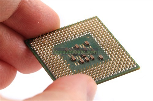
What is Megtron 8 Substrate?
메그트론 8 is a high-performance PCB substrate primarily used for high-speed and high-frequency electronic applications. This material was developed by the Japanese company Megtron and possesses excellent electrical and mechanical properties, meeting the increasingly stringent requirements of modern electronic products.
메그트론 8 substrates are made from a special resin material with a low dielectric constant and low loss factor, which ensures outstanding performance in high-frequency signal transmission. Compared to traditional FR-4 materials, 메그트론 8 has better thermal stability and a lower coefficient of thermal expansion, effectively reducing structural deformation caused by temperature fluctuations. This characteristic is crucial for high-frequency circuit design, as even minor changes can significantly impact signal integrity during high-speed operations.
또한, 메그트론 8 exhibits superior chemical resistance and moisture absorption rates, maintaining stable performance even in harsh environments. This substrate is widely used in communication devices, computer hardware, industrial automation, and automotive electronics.
요약하면 다음과 같습니다, 메그트론 8 has become an ideal choice for high-frequency and high-speed PCB design due to its exceptional electrical properties and superior mechanical performance, adapting to the rapid advancements in modern electronic technology.

메그트론 8 기판 제조업체
What is the Megtron 8 Substrate Design Guidelines?
The design guidelines for 메그트론 8 기판 focus on optimizing performance in high-frequency and high-speed applications. Here are some key considerations:
- 레이어 스택업: Ensure proper layer arrangement to minimize signal loss and maintain impedance control. Use microstrip or stripline configurations as needed.
- 트레이스 폭 및 간격: Calculate trace widths carefully to maintain desired impedance levels. Pay attention to spacing between traces to avoid crosstalk.
- 비아 디자인: Use blind and buried vias where possible to reduce inductance and improve signal integrity. Keep via diameters small to minimize parasitic capacitance.
- 그라운드 플레인: Utilize continuous ground planes to reduce electromagnetic interference (EMI (이엠아이)) and improve return paths for high-speed signals.
- 열 관리: Consider thermal dissipation, 특히 고출력 응용 분야에서. Use thermal vias and pads strategically to enhance heat dissipation.
- Simulation Tools: Employ high-frequency simulation tools (like HFSS or ADS) during the design phase to validate signal integrity and electromagnetic performance.
- 제조 공차: Be aware of the manufacturing capabilities and tolerances of the substrate. Collaborate with manufacturers early in the design process to ensure feasibility.
- 테스트 및 검증: Plan for appropriate testing methods, including TDR (Time Domain Reflectometry) and S-parameter measurements, to validate design performance post-manufacturing.
이 지침을 준수함으로써, designers can leverage the full capabilities of Megtron 8 substrates for reliable high-frequency and high-speed circuit performance.
The advantages of Megtron 8 Substrate
메그트론 8 기판 offer several advantages, particularly suited for high-frequency and high-speed applications:
- Low Dielectric Constant: This property ensures minimal signal loss, enhancing signal integrity in high-speed circuits.
- Low Loss Factor: The substrate minimizes energy loss during signal transmission, which is crucial for maintaining performance in high-frequency applications.
- High Thermal Stability: 메그트론 8 can withstand higher temperatures, reducing the risk of deformation and maintaining performance in demanding environments.
- Low Coefficient of Thermal Expansion: This helps in maintaining dimensional stability, reducing warping and stress during thermal cycling.
- Excellent Moisture Resistance: The substrate’s low moisture absorption rates prevent degradation in performance, particularly in humid conditions.
- Superior Chemical Resistance: It can withstand various chemicals, making it suitable for applications in harsh environments.
- Robust Mechanical Properties: 메그트론 8 provides good mechanical strength, which aids in durability during handling and assembly.
- Versatility: It is suitable for a wide range of applications, 통신 포함, 컴퓨팅, 자동차, 및 산업용 전자 제품.
These advantages make Megtron 8 a preferred choice for engineers designing high-performance electronic systems.
What is the Megtron 8 Substrate Fabrication Process?
The fabrication process for Megtron 8 substrates involves several key steps, ensuring high precision and quality suitable for high-frequency applications:
- 재료 준비: Begin with the raw Megtron 8 material, which is a type of epoxy resin with specialized fillers. This material is available in sheets of varying thicknesses.
- Layer Cutting: Cut the Megtron 8 sheets to the required dimensions based on the design specifications.
- Copper Lamination: Bond copper foil to the surface of the substrate using heat and pressure. This is typically done in a lamination press to ensure a strong adhesion.
- Photo-Plotting: Apply a photoresist layer to the copper surface, followed by exposure to ultraviolet light through a photomask. This process defines the circuit patterns.
- Developing: After exposure, the photoresist is developed, removing the unexposed areas and leaving the desired circuit pattern on the copper layer.
- 에칭: The exposed copper is chemically etched away, leaving the circuit traces intact on the substrate.
- 드릴링: Holes for vias and component leads are drilled using precision drilling equipment. This step must be carefully controlled to maintain integrity.
- Via Plating: If necessary, vias are plated with copper to create electrical connections between layers. This step may involve electroplating or chemical plating processes.
- Final Finishing: Additional processes, such as surface treatments or applying solder masks, may be applied to enhance performance and durability.
- Testing:Conduct rigorous testing to ensure electrical integrity and adherence to design specifications, including tests for impedance, 신호 무결성, 및 열적 특성.
By following these fabrication steps, manufacturers can produce high-quality Megtron 8 substrates that meet the demanding requirements of modern electronic applications.
The application of ceramic Megtron 8 Substrate
Ceramic Megtron 8 substrates are used in various applications due to their superior electrical and mechanical properties. 다음은 몇 가지 주요 응용 프로그램입니다:
- 통신: Used in high-speed communication devices, such as routers and switches, where signal integrity is critical.
- 소비자 가전제품: Found in smartphones, 정제, 그리고 게임 콘솔, where compact design and high performance are required.
- 자동차 전장: Used in advanced driver-assistance systems (ADAS (장애인)) and electric vehicle components, providing reliability in harsh environments.
- Industrial Automation: Employed in control systems and sensors, offering durability and performance in industrial settings.
- 항공우주 및 방위 산업: Utilized in avionics and military communications, where high reliability and performance under extreme conditions are essential.
- 의료 기기: Implemented in diagnostic and monitoring equipment, ensuring precision and reliability in critical applications.
These applications leverage the thermal stability, low loss, and mechanical strength of Megtron 8 기판, making them ideal for demanding electronic environments.
FAQs about Megtron 8 Substrate
What is Megtron 8?
메그트론 8 is a high-performance PCB substrate designed for high-frequency and high-speed electronic applications, offering low dielectric constant and loss.
What are the main advantages of Megtron 8?
Key advantages include low signal loss, high thermal stability, low moisture absorption, and superior mechanical properties, making it ideal for demanding environments.
In which applications is Megtron 8 commonly used?
It is used in telecommunications, 소비자 가전제품, automotive systems, industrial automation, 항공 우주, 방어, 및 의료 기기.
How does Megtron 8 compare to traditional FR-4 substrates?
메그트론 8 offers better performance at high frequencies, lower loss, improved thermal stability, and greater reliability in harsh conditions compared to FR-4.
What is the fabrication process for Megtron 8 기판?
제작 공정에는 재료 준비가 포함됩니다, copper lamination, photo-plotting, 에칭, 드릴링, via plating, and final finishing.
Can Megtron 8 substrates be used in multilayer designs?
예, 메그트론 8 substrates are suitable for multilayer designs, offering excellent performance and reliability across multiple layers.
What testing methods are used for Megtron 8 기판?
Common testing methods include Time Domain Reflectometry (TDR), S-parameter measurements, and thermal cycling tests to ensure performance and reliability.
Are there specific design guidelines for Megtron 8?
예, design guidelines include considerations for layer stackup, trace width and spacing, via design, ground plane usage, and thermal management.


) 세라믹 기판 제조업체")
