
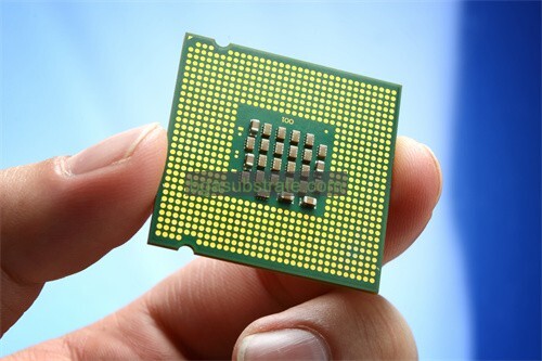
Megtron 7N Substrate 생산자
Megtron 7N 기판 제조업체,Megtron 7N substrate is a high-performance material specifically designed for advanced electronic applications. Known for its excellent thermal conductivity and low dielectric constant, it provides superior electrical performance in high-frequency circuits. Megtron 7N features low moisture absorption and high dimensional stability, which enhance its reliability in demanding environments. Its unique resin formulation allows for fine line processing, making it suitable for multilayer circuit boards and high-density interconnects. 또한, the substrate is compatible with various manufacturing processes, enabling efficient production of complex electronic assemblies. Megtron 7N is widely used in telecommunications, 자동차, 및 항공우주 응용 분야, where performance is critical.
What is Megtron 7N Substrate?
Megtron 7N substrate is a high-performance printed circuit board material designed for high-frequency and high-speed applications. Developed by Japan’s Megtron company, it employs a range of advanced materials and processes, resulting in excellent electrical performance and mechanical strength in electronic devices.
The key features of Megtron 7N substrate include low dielectric constant (디케이) 그리고 낮은 손실 계수 (디에프), making it particularly suitable for high-speed signal transmission applications, such as communication devices, 레이더 시스템, and high-frequency microwave equipment. 또한, Megtron 7N exhibits excellent thermal stability and chemical resistance, allowing it to maintain good performance in high-temperature and harsh environments.
This substrate also offers good processing characteristics, making it easy to bond with other materials, such as copper layers and surface-mount components, facilitating its use in complex circuit designs. Due to its outstanding electrical and mechanical properties, Megtron 7N is widely used in high-end consumer electronics, 컴퓨팅, and automotive electronics, meeting the stringent demands for performance and reliability in modern electronic products.
요약하면 다음과 같습니다, Megtron 7N substrate is an ideal choice for high-frequency and high-speed applications, and its superior electrical performance and reliability make it a preferred material in many high-tech industries.

Megtron 7N 기판 제조업체
What is the Megtron 7N Substrate Design Guidelines?
The design guidelines for Megtron 7N substrate typically focus on optimizing performance for high-frequency and high-speed applications. Here are some key considerations:
- 레이어 스택업: Design the layer stackup to minimize signal integrity issues. Consider using controlled impedance layers for high-speed signals.
- 트레이스 폭 및 간격: Calculate trace width and spacing to achieve the desired impedance. Use design tools to ensure proper dimensions based on the substrate’s dielectric properties.
- 비아 디자인: Use microvias or blind/buried vias where possible to reduce inductance and enhance signal integrity. Ensure proper plating and finish for reliability.
- 열 관리: Incorporate thermal vias and pads to manage heat dissipation, especially for power components. Consider copper pours for better heat spreading.
- Signal Routing: Keep high-speed signals short and direct. Avoid sharp angles and unnecessary vias to minimize reflections and losses.
- Grounding: 전자기 간섭을 줄이기 위해 견고한 접지면을 활용하십시오. (EMI (이엠아이)) and enhance performance. Ensure proper grounding for signal return paths.
- Layer Separation: Maintain adequate separation between power and signal layers to reduce noise coupling.
- Manufacturing Considerations: Follow the manufacturer’s recommendations for hole sizes, edge clearance, and surface finishes to ensure manufacturability and reliability.
- 테스트 및 검증:Plan for signal integrity analysis and thermal testing during the design phase to validate performance under operating conditions.
이 지침을 준수함으로써, designers can optimize the performance of Megtron 7N substrates in demanding electronic applications.
The advantages of Megtron 7N Substrate
Megtron 7N substrate offers several advantages, particularly for high-frequency and high-speed applications:
- Low Dielectric Constant (디케이): This feature allows for reduced signal propagation delays, making it ideal for high-speed digital and RF applications.
- Low Dissipation Factor (디에프): The low Df contributes to minimal signal loss, improving overall performance in high-frequency circuits.
- 열 안정성: Megtron 7N exhibits excellent thermal properties, maintaining performance in high-temperature environments, which is essential for reliability in demanding applications.
- 내화학성: The substrate is resistant to various chemicals, enhancing durability and longevity in different operating conditions.
- 기계적 강도: It offers good mechanical properties, providing robustness and stability during manufacturing and end-use.
- Good Processing Characteristics:Megtron 7N is compatible with standard PCB fabrication processes, facilitating easier design and manufacturing.
- Excellent Impedance Control: The substrate supports precise impedance matching, which is crucial for maintaining signal integrity in high-speed applications.
- Versatility: Suitable for a wide range of applications, 통신 포함, 자동차, 및 소비자 전자 제품, making it a versatile choice for designers.
These advantages make Megtron 7N a preferred material for manufacturers seeking high performance and reliability in electronic products.
What is the Megtron 7N Substrate Fabrication Process?
The fabrication process of Megtron 7N substrate generally involves several key steps, similar to standard PCB manufacturing but tailored for its specific material properties. Here’s an overview:
- 재료 준비: Megtron 7N sheets are cut to the desired size and prepared for lamination. The substrate is typically made of a glass-reinforced epoxy material designed for high-frequency applications.
- Layering: If the design includes multiple layers, the layers are stacked according to the required stackup configuration. This may involve adding prepreg layers between core layers.
- 박판: The stacked layers are subjected to heat and pressure in a lamination process, which cures the resin and bonds the layers together. This step is critical for ensuring mechanical stability and electrical performance.
- 드릴링: 적층 후, holes are drilled for vias and mounting holes. The drilling process needs to be precise to avoid damaging the substrate and to maintain the integrity of high-frequency signals.
- 구리 도금: The drilled holes are plated with copper to create conductive pathways. This can involve electroless copper plating followed by electrolytic plating to achieve the desired thickness.
- 에칭: The copper layers are etched to create the desired circuit patterns. 여기에는 포토레지스트 층을 적용하는 것이 포함됩니다, exposing it to UV light, and then etching away unprotected copper.
- 표면 마감: A surface finish is applied to protect the copper and improve solderability. Common finishes include immersion gold, HASL, or ENEPIG, depending on the application requirements.
- 테스트 및 검사: The fabricated substrates undergo electrical testing, 육안 검사, and other quality control measures to ensure they meet specified performance standards.
- Final Cutting and Packaging: Once testing is complete, the substrates are cut to the final dimensions and packaged for shipment.
These steps are designed to optimize the unique properties of Megtron 7N, ensuring high performance in applications that demand reliability and speed.
The application of ceramic Megtron 7N Substrate
Megtron 7N substrate, despite its name sounding like a ceramic, is actually a high-performance epoxy-based printed circuit board material, 세라믹 기판이 아님. It’s specifically designed for high-frequency and high-speed applications in electronic devices. Here are some typical applications:
- 통신: Used in base stations, 안테나, and other communication equipment where high-frequency performance is critical.
- Data Communications: Employed in routers, 스위치, servers, and other networking equipment for efficient data transmission.
- 항공우주 및 방위 산업: Used in radar systems, 항공, and satellite communication equipment due to its reliability under extreme conditions and high-speed signal capabilities.
- 자동차 전장: Found in advanced driver-assistance systems (ADAS (장애인)), infotainment systems, 및 엔진 제어 장치 (ECU (영문)) where durability and signal integrity are crucial.
- 소비자 가전제품: Used in high-end smartphones, 정제, and other portable devices where compact size and high performance are required.
- 산업용 전자 제품: Applied in automation equipment, 제어 시스템, and sensors where robustness and reliability are essential.
- 의료 기기: Utilized in diagnostic equipment, 이미징 시스템, and medical monitors for reliable signal processing and data transmission.
Megtron 7N substrate’s advantages, such as low dielectric constant, low dissipation factor, excellent thermal stability, 및 기계적 강도, make it suitable for demanding applications where high-frequency performance and reliability are paramount.
FAQs about Megtron 7N Substrate
What is Megtron 7N substrate made of?
Megtron 7N substrate is primarily made of glass-reinforced epoxy material, specifically designed for high-frequency and high-speed applications.
What are the main advantages of using Megtron 7N?
Key advantages include low dielectric constant (디케이), low dissipation factor (디에프), excellent thermal stability, good mechanical strength, and high chemical resistance, making it ideal for demanding electronic applications.
In which applications is Megtron 7N typically used?
It is commonly used in telecommunications, data communications, 항공우주 및 방위 산업, 자동차 전자 장치, 소비자 가전제품, 산업용 전자 제품, 및 의료 기기.
How does Megtron 7N compare to traditional FR-4 substrates?
Megtron 7N offers superior performance at high frequencies and speeds compared to traditional FR-4 substrates, particularly in terms of signal integrity and thermal stability.
Can Megtron 7N be used in multilayer PCB designs?
예, Megtron 7N is suitable for multilayer PCB designs, supporting complex layouts and impedance-controlled designs.
What is the fabrication process for Megtron 7N substrates?
제작 공정에는 재료 준비가 포함됩니다, 레이어 링, 박판, 드릴링, 구리 도금, 에칭, applying surface finishes, and testing.
Is Megtron 7N compatible with standard PCB manufacturing processes?
예, it is compatible with most standard PCB manufacturing processes, although some specific considerations may be needed due to its unique properties.
What kind of testing is recommended for Megtron 7N substrates?
Electrical testing, thermal testing, and visual inspection are recommended to ensure performance and reliability.


) 세라믹 기판 제조업체")
