
Hybrid Ceramic Substrate 생산자
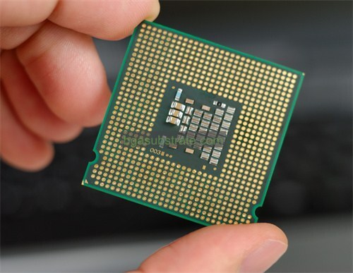
하이브리드 세라믹 기판 제조업체,Hybrid Ceramic Substrate combines the advantages of ceramic and organic materials in electronic packaging. It typically consists of a ceramic base layer for robustness and thermal management, with organic layers for interconnections and flexibility. This substrate enables high-density integration of components while maintaining reliability and performance in demanding environments. Hybrid ceramic substrates are pivotal in advanced applications such as automotive electronics, 항공우주 시스템, and telecommunications infrastructure, where they provide excellent electrical insulation, thermal dissipation, 및 기계적 강도, crucial for ensuring the longevity and efficiency of electronic devices.
무엇입니까 Hybrid Ceramic Substrate?
A hybrid ceramic substrate is a type of material used primarily in electronics for packaging and integrating semiconductor devices. It combines the properties of ceramics and metals to achieve optimal performance in terms of electrical insulation, 열전도율, 및 기계적 강도.
These substrates are typically composed of a ceramic base material, such as alumina (알2O3) 또는 질화알루미늄 (알엔(AlN)), which provides excellent electrical insulation and thermal conductivity. On top of this ceramic base, thin layers of conductive metals like copper or tungsten are deposited using various techniques like sputtering or thick-film printing. These metal layers form the circuit paths and interconnections required for electronic components.
The hybrid nature of these substrates allows them to handle high-power applications efficiently by dissipating heat effectively through the ceramic base while providing robust mechanical support through the metal layers. This makes them suitable for use in power modules, LED packages, 마이크로파 장치, and other electronics where reliability and performance under demanding conditions are crucial.
요약하면 다음과 같습니다, a hybrid ceramic substrate is a specialized material designed to leverage the strengths of ceramics and metals, offering a balanced combination of electrical insulation, 열 관리, and mechanical stability essential for advanced electronic applications.

하이브리드 세라믹 기판 제조업체
무엇입니까 Hybrid Ceramic Substrate 디자인 지침?
에 대한 디자인 지침 hybrid ceramic substrates focus on optimizing their performance and reliability in electronic applications. Here are some key considerations:
- 재료 선택: Choose appropriate ceramic materials based on thermal conductivity (예), alumina, aluminum nitride) 및 기계적 강도. The choice depends on the specific requirements of heat dissipation and mechanical support for the components.
- 레이어 구성: Determine the optimal configuration of ceramic and metal layers. 일반적 으로, ceramic substrates have multiple layers where each layer serves a specific function such as electrical insulation or thermal management.
- 열 관리: Design effective thermal paths to ensure efficient heat dissipation from heat-generating components to the substrate and then to the external environment. This involves proper placement of vias, 히트 스프레더, and thermal vias to minimize thermal resistance.
- Electrical Performance: Ensure low electrical losses and proper impedance matching by designing appropriate conductor widths and thicknesses. This is crucial for maintaining signal integrity and minimizing electromagnetic interference (EMI (이엠아이)).
- 기계적 고려 사항: Design the substrate to withstand mechanical stresses during assembly, operation, and thermal cycling. Consider factors like coefficient of thermal expansion (증권 시세 표시기) matching with components and mounting surfaces to prevent mechanical failures.
- Reliability and Durability: Design for long-term reliability by considering factors such as solder joint integrity, thermal cycling resistance, and resistance to environmental factors like humidity and temperature variations.
- 제조 가능성: Ensure that the substrate design is manufacturable within acceptable tolerances and cost-effective. Consider the capabilities of fabrication techniques such as screen printing, laser processing, and metallization.
- Integration with Components: Design the substrate to facilitate easy integration with semiconductor devices, passive components, and other electronic elements. This includes optimizing pad layouts, alignment features, and connection points.
- Testing and Quality Assurance: Define testing protocols to validate the substrate’s electrical, 열, and mechanical performance before deployment in the final electronic assembly. This helps ensure consistent quality and performance.
- Documentation and Standards Compliance: Document the design guidelines and adhere to relevant industry standards (예), IPC standards for PCBs) to ensure compatibility, 신뢰도, and safety in the intended application.
다음 디자인 지침을 따릅니다, engineers can optimize the performance, 신뢰도, and manufacturability of hybrid ceramic substrates for various electronic applications ranging from power electronics to high-frequency communication devices.
의 장점 Hybrid Ceramic Substrate
Hybrid ceramic substrates offer several advantages that make them desirable for various electronic applications:
- 열 관리:They provide excellent thermal conductivity due to the ceramic base material (예), alumina, aluminum nitride), which efficiently dissipates heat away from components. This capability is crucial for high-power applications where heat generation is significant.
- 전기 절연: Ceramic substrates inherently offer high electrical insulation properties, preventing leakage currents and ensuring the reliability of electrical connections even at high voltages.
- 기계적 강도: The combination of ceramic and metal layers provides robust mechanical support for components. This strength helps withstand mechanical stresses during assembly, operation, and thermal cycling, reducing the risk of mechanical failure.
- 소형화: Hybrid ceramic substrates allow for compact designs and integration of multiple components in a smaller space. This is advantageous in applications where size and weight are critical factors.
- 고주파 성능: They exhibit excellent high-frequency characteristics, making them suitable for use in RF (무선 주파수) 그리고 마이크로파 응용(microwave applications). The low dielectric losses of ceramic materials enable efficient signal transmission without significant degradation.
- Customizability: Hybrid ceramic substrates can be customized in terms of material composition, layer configuration, and layout design to meet specific performance requirements of different electronic devices and circuits.
- 호환성: They are compatible with various assembly and packaging techniques, including soldering, 와이어 본딩, and flip-chip bonding, facilitating ease of integration into electronic assemblies.
- Reliability: Due to their stable material properties and robust design, hybrid ceramic substrates offer high reliability and long-term performance consistency, critical for applications demanding continuous operation and minimal downtime.
- Environmental Resistance: Ceramic materials are inherently resistant to environmental factors such as moisture, chemicals, and temperature variations, enhancing the substrate’s durability in harsh operating conditions.
- 비용 효율성: While initial manufacturing costs can vary, hybrid ceramic substrates often provide cost savings in the long run due to their reliability and reduced need for cooling systems or additional components to manage heat dissipation.
전반적, the advantages of hybrid ceramic substrates make them preferred choices for applications where thermal management, 전기 절연, 기계적 강도, and high-frequency performance are crucial requirements.
무엇입니까 Hybrid Ceramic Substrate 제작 과정?
The fabrication process of hybrid ceramic substrates involves several key steps to achieve the desired material properties and functionality:
- 재료 선택: Choose ceramic materials based on application requirements such as thermal conductivity, 전기 절연, 및 기계적 강도. Common ceramics used include alumina (알2O3) 및 질화 알루미늄 (알엔(AlN)).
- Substrate Preparation: Start with a ceramic base substrate typically in the form of sheets or panels. These substrates are prepared by cutting or machining to the required dimensions.
- 금속: Apply conductive metal layers onto the ceramic substrate. This step is crucial for creating circuit paths, interconnections, and bonding pads. Metallization can be achieved through techniques like screen printing, thin-film deposition (스퍼터 링), or thick-film printing using pastes containing metals such as silver, 금, or copper.
- Pattern Definition: Define the specific circuit patterns and features using photolithography or screen printing techniques. This involves applying a photoresist layer over the metallized substrate, 마스크를 통해 자외선에 노출시키는 경우, and then developing it to create the desired conductor patterns.
- 발사: Heat treat the substrate in a furnace to sinter the ceramic material and bond the metal layers securely. This firing process ensures strong adhesion between the ceramic and metal layers while enhancing the electrical and mechanical properties of the substrate.
- 포메이션을 통해: Create vias (vertical interconnect access) to establish electrical connections between different layers of the substrate. Vias are typically formed by drilling or laser ablation followed by filling with conductive material such as copper or tungsten.
- 표면 마무리: Apply surface finishes to the substrate to enhance solderability and protect the metallized layers from oxidation. Common surface finishes include gold plating or tin-lead solder.
- Testing and Quality Control: Perform rigorous testing to verify the electrical continuity, insulation resistance, 열전도율, and mechanical strength of the fabricated substrates. This ensures that they meet the specified performance criteria and reliability standards.
- Assembly and Packaging: After fabrication, hybrid ceramic substrates are ready for assembly with semiconductor devices, passive components, and other electronic elements. They are integrated using standard assembly processes like soldering or bonding techniques.
- Documentation and Traceability: Maintain detailed documentation throughout the fabrication process to ensure traceability and compliance with industry standards. This documentation includes material specifications, process parameters, and quality control records.
By following these fabrication steps meticulously, manufacturers can produce hybrid ceramic substrates that offer superior thermal management, 전기 절연, 기계적 강도, and reliability for a wide range of electronic applications.
세라믹의 적용 Hybrid Ceramic Substrate
Hybrid ceramic substrates find application in various electronic and semiconductor industries due to their unique combination of thermal conductivity, 전기 절연, 기계적 강도, 그리고 신뢰성. 일부 주요 응용 프로그램은 다음과 같습니다:
- 파워 일렉트로닉스: Hybrid ceramic substrates are extensively used in power electronic modules such as insulated gate bipolar transistors (IGBT), power diodes, and thyristors. Their excellent thermal conductivity helps in efficient heat dissipation, which is critical for handling high-power densities and maintaining device reliability.
- LED Packaging: They are employed in LED (light-emitting diode) packaging to provide thermal management for LEDs. Hybrid ceramic substrates help in dissipating heat generated by LEDs, thereby extending their lifespan and improving overall efficiency.
- RF/Microwave Devices: Due to their low dielectric losses and high-frequency performance, hybrid ceramic substrates are ideal for RF (무선 주파수) 그리고 마이크로파 응용(microwave applications). They are used in components such as filters, 증폭기, 안테나, and resonators where maintaining signal integrity and minimizing losses are crucial.
- 자동차 전장: 자동차 응용 분야에서, hybrid ceramic substrates are used in powertrain control modules, 엔진 제어 장치 (ECU (영문)), and electric vehicle (EV) 인버터. Their ability to withstand high temperatures, mechanical stresses, and vibrations makes them suitable for harsh automotive environments.
- Communication Systems: They are integral in communication systems including base stations, satellite communication equipment, and wireless routers. Hybrid ceramic substrates support the performance requirements of high-speed data transmission and signal processing.
- 의료 전자 장치: 의료 기기 및 장비에서, hybrid ceramic substrates contribute to reliable operation and longevity. They are used in devices such as implantable medical devices, 진단 장비, and patient monitoring systems where precision, 내구성, and biocompatibility are essential.
- Industrial Automation: Hybrid ceramic substrates play a role in industrial automation applications such as motor drives, 로봇공학, and control systems. Their robust construction and thermal management capabilities ensure stable operation in industrial environments.
- 소비자 가전제품: They find application in consumer electronics products such as smartphones, 정제, and wearable devices where miniaturization, thermal efficiency, and reliability are critical factors.
요약하면 다음과 같습니다, the application of hybrid ceramic substrates spans a wide range of industries and technologies where their unique combination of properties addresses challenges related to thermal management, 전기 절연, 기계적 견고성, and high-frequency performance in electronic systems and devices.
에 대한 FAQ Hybrid Ceramic Substrate
What is a hybrid ceramic substrate?
A hybrid ceramic substrate is a material used in electronics that combines ceramic and metal layers. It provides excellent thermal conductivity, 전기 절연, 및 기계적 강도, making it ideal for applications requiring efficient heat dissipation and reliable electrical performance.
What are the advantages of using hybrid ceramic substrates?
Hybrid ceramic substrates offer advantages such as superior thermal management, high electrical insulation, strong mechanical support, compatibility with high-frequency applications, 열악한 환경에서의 신뢰성. They are also customizable and support miniaturization.
What are hybrid ceramic substrates used for?
They are used in various electronic applications including power electronics (IGBT, 전력 모듈), LED packaging, RF/마이크로파 장치 (안테나, 증폭기), 자동차 전자 장치 (ECU (영문), EV inverters), 통신 시스템 (기지국, routers), 의료 기기, 및 소비자 전자 제품.
How are hybrid ceramic substrates fabricated?
Fabrication involves selecting ceramic materials like alumina or aluminum nitride, metallizing the substrate with conductive metals (예), 은, 구리), defining circuit patterns via photolithography, firing to sinter the layers, forming vias for interconnections, and applying surface finishes for solderability and protection.
What are the key considerations in designing hybrid ceramic substrates?
Design considerations include material selection for thermal conductivity and mechanical strength, optimizing layer configuration for electrical performance, ensuring effective thermal management, designing for reliability and durability, and complying with industry standards for manufacturability.
Are hybrid ceramic substrates expensive?
Initial manufacturing costs can vary, but hybrid ceramic substrates often provide cost savings in the long run due to their reliability, reduced need for additional cooling systems, and extended operational lifespan in high-demand applications.
What industries benefit from using hybrid ceramic substrates?
Industries such as electronics, 반도체 제조, 자동차, 통신, 항공 우주, 의료 기기, and industrial automation benefit from the unique properties of hybrid ceramic substrates in their products and systems.
 기판 제조업체")
 세라믹 기판 제조업체")
 세라믹 기판 제조업체")
) 세라믹 기판 제조업체")
 세라믹 기판 제조업체")


