
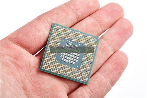
FCLGA Substrate 생산자
FCLGA 기판 제조업체,FCLGA (Flip Chip Land Grid Array) substrates are sophisticated packaging solutions used in semiconductor devices where the chip is mounted face-down and connected via solder bumps. 이 “land grid array” configuration features a grid of flat metal pads on the substrate, which interface with the solder bumps on the chip. This design allows for high-density interconnections, 우수한 전기적 성능, and effective thermal management. FCLGA substrates are ideal for high-performance applications, 프로세서 포함, 그래픽 카드, and memory modules. They support high-speed data transfer and offer enhanced reliability and robustness, making them essential for advanced electronic systems and demanding computing environments.
무엇입니까 FCLGA Substrate?
FCLGA (Flip-Chip Land Grid Array) substrates are advanced interconnect solutions used primarily in high-performance integrated circuits. They provide a critical interface between a semiconductor chip and the printed circuit board (폴리염화비페). The FCLGA package is distinguished by its use of a flip-chip configuration, where the chip is mounted upside down, with its active surface facing the substrate. This allows for high-density interconnection and better thermal performance.
The FCLGA substrate features a land grid array (LGA) design, where the connections to the PCB are made through an array of lands or pads rather than traditional pins. This land grid array provides a larger surface area for electrical contacts, enhancing the reliability of the connections and reducing the overall footprint of the package.
The key advantages of FCLGA substrates include improved signal integrity, 감소된 인덕턴스 및 커패시턴스, and enhanced heat dissipation. These properties make FCLGA substrates ideal for high-speed and high-frequency applications such as processors, 메모리 모듈, and advanced communication devices. 또한, FCLGA substrates are often used in applications requiring high-performance computing and consumer electronics where thermal management and signal integrity are critical.
요약하면 다음과 같습니다, the FCLGA substrate is a sophisticated packaging technology that leverages the benefits of flip-chip assembly and land grid array design to support high-performance, high-density electronic devices, ensuring efficient electrical connectivity and effective thermal management.

FCLGA 기판 제조업체
무엇입니까 FCLGA Substrate 디자인 지침?
FCLGA (Flip-Chip Land Grid Array) 기판 design guidelines are crucial for ensuring optimal performance, 신뢰도, and manufacturability of the package. Here are some key considerations:
- 열 관리: Effective heat dissipation is essential in FCLGA substrates due to high power densities. Design guidelines should include thermal vias and heat spreaders to ensure that heat is efficiently transferred away from the chip. Considerations for the substrate’s thermal conductivity and the placement of thermal pads are critical to managing heat effectively.
- 신호 무결성: High-speed and high-frequency applications require careful management of signal integrity. This involves designing for controlled impedance, minimizing signal traces’ length, and avoiding sharp corners. It’s also important to include adequate grounding and power planes to reduce noise and interference.
- 패드 및 비아 디자인: The layout of lands or pads must match the chip’s contact pattern precisely. Vias should be designed to support high current loads and to minimize inductance and capacitance. The pad size and spacing should adhere to the manufacturer’s specifications to ensure proper soldering and electrical performance.
- 기계적 고려 사항: The substrate must support the mechanical stress associated with the flip-chip assembly process. This involves designing for proper mechanical strength and ensuring that the substrate can withstand the thermal cycling that occurs during operation.
- Manufacturability and Reliability: The design should consider the manufacturing processes, such as solder mask application and the potential for warpage. Reliability testing, such as thermal cycling and mechanical stress testing, should be included in the design phase to ensure the substrate performs reliably over its expected lifespan.
- Electrical Performance: To enhance electrical performance, ensure the substrate supports the required electrical characteristics, including low resistance and low inductance. This involves careful consideration of material choices and layer stack-ups to meet the performance specifications.
요약하면 다음과 같습니다, FCLGA substrate design guidelines emphasize thermal management, 신호 무결성, precise pad and via design, 기계적 견고성, manufacturability, and electrical performance. Following these guidelines ensures that FCLGA packages meet the high-performance demands of modern electronic devices.
의 장점 FCLGA Substrate
FCLGA (Flip-Chip Land Grid Array) 기판 offer several advantages that make them highly suitable for advanced electronic applications. 주요 이점은 다음과 같습니다:
- Enhanced Thermal Performance: FCLGA substrates are designed with effective heat dissipation features, such as thermal vias and heat spreaders. This helps in managing heat generated by high-performance chips, ensuring reliable operation and reducing the risk of thermal-related failures.
- High-Density Interconnection: The flip-chip configuration allows for a higher density of interconnections compared to traditional pin-grid array packages. This compact design enables more connections in a smaller footprint, which is crucial for high-performance and space-constrained applications.
- 향상된 전기적 성능: By using a flip-chip assembly, FCLGA substrates minimize the distance between the chip and the substrate, reducing signal path lengths. This leads to lower inductance and capacitance, enhancing signal integrity and enabling higher-speed operation.
- 축소된 패키지 크기: The land grid array design allows for a more compact package compared to other types of arrays with protruding pins. This reduction in size helps in achieving more compact and lightweight electronic devices, which is beneficial for mobile and consumer electronics.
- Better Mechanical Stability: FCLGA substrates offer improved mechanical stability due to their robust design. The direct contact of the chip’s active surface with the substrate enhances the mechanical connection, providing greater resistance to physical stress and mechanical shock.
- Simplified Assembly Process: The land grid array approach simplifies the assembly process by using a grid of lands rather than individual pins. This can lead to more reliable soldering and reduced assembly time, contributing to overall cost savings.
- 향상된 신뢰성: The combination of flip-chip mounting and land grid array design contributes to higher package reliability. The reduction in mechanical stress and improved thermal and electrical performance ensures that FCLGA substrates can withstand demanding operational conditions.
요약하면 다음과 같습니다, FCLGA substrates offer significant advantages in terms of thermal management, interconnection density, 전기적 성능, package size, 기계적 안정성, assembly efficiency, 그리고 신뢰성. These benefits make them an excellent choice for high-performance electronic applications requiring efficient and compact packaging solutions.
무엇입니까 FCLGA Substrate 제작 과정?
The FCLGA (Flip-Chip Land Grid Array) substrate fabrication process involves several key steps to produce a high-performance, reliable substrate for advanced electronic packaging. 다음은 일반적인 제조 공정에 대한 개요입니다:
- 기판 재료 준비: The fabrication begins with selecting and preparing the substrate material, typically a laminate made from materials such as epoxy resin, glass fiber, or polyimide. The choice of material affects the substrate’s thermal and electrical properties.
- Copper Clad Laminate: The substrate material is often laminated with copper foil on one or both sides. This copper layer serves as the base for the circuit routing and pad formation. The copper foil is bonded to the laminate using heat and pressure.
- 3. 포토리소그래피: A photoresist layer is applied to the copper surface. Photolithography is used to pattern the copper layer by exposing it to UV light through a mask that defines the desired circuit layout. 노출된 포토레지스트가 개발되었습니다., removing the photoresist from areas that need to be etched away.
- 에칭:The exposed copper is etched away using a chemical etching process, leaving behind the circuit patterns and land grid array pads. This process creates the necessary electrical connections and patterns on the substrate.
- 포메이션을 통해: 비아, which are vertical conductive paths connecting different layers of the substrate, are drilled or laser-machined into the substrate. These vias are then plated with copper to ensure electrical connectivity between layers.
- 솔더 마스크 적용: A solder mask layer is applied to protect the circuit patterns and define the areas where solder will be applied. The solder mask is typically green and helps to prevent solder bridging and accidental short circuits.
- Pad Plating: The exposed pads on the substrate are plated with a thin layer of metal, such as gold or nickel, to enhance solderability and improve the reliability of electrical connections.
- Chip Placement and Soldering: The flip-chip die is positioned onto the substrate with its active surface facing down. Solder bumps or balls on the chip align with the substrate’s land grid array pads. Reflow soldering is used to melt the solder and create permanent electrical connections between the chip and the substrate.
- 캡슐화 및 테스트: After soldering, the assembly may be encapsulated with an underfill material to protect the solder joints and enhance mechanical stability. 마침내, the substrate undergoes rigorous testing to ensure it meets performance and reliability standards.
- 최종 검사 및 포장: The completed FCLGA substrate is inspected for defects, and any necessary adjustments are made. It is then packaged for shipment to customers or for further integration into electronic devices.
요약하면 다음과 같습니다, the FCLGA substrate fabrication process involves substrate material preparation, copper lamination, 포토리소그래피, 에칭, 포메이션을 통해, 솔더 마스크 적용, pad plating, chip placement and soldering, encapsulation, 테스트, and final inspection. Each step is crucial for ensuring the substrate meets the performance and reliability requirements of high-end electronic applications.
세라믹의 적용 FCLGA Substrate
Ceramic FCLGA (Flip-Chip Land Grid Array) substrates are utilized in a variety of advanced electronic applications due to their superior properties compared to traditional organic substrates. Here are the key applications:
- High-Performance Processors: Ceramic FCLGA substrates are widely used in high-performance processors, including CPUs and GPUs. Their excellent thermal conductivity helps manage heat dissipation effectively, which is crucial for maintaining performance and reliability in high-power computing applications.
- Memory Modules: In memory modules, such as high-speed DRAM and SRAM, ceramic FCLGA substrates provide the necessary electrical and thermal properties to support fast data transfer rates and reliable operation. Their high-density interconnection capabilities also contribute to improved performance and compact design.
- RF 및 마이크로웨이브 애플리케이션: For radio frequency (무선 주파수 (RF)) 그리고 마이크로파 응용(microwave applications), ceramic FCLGA substrates are preferred due to their low dielectric loss and stable electrical performance at high frequencies. They are used in components like RF amplifiers, oscillators, and filters, where maintaining signal integrity is critical.
- Telecommunications Equipment: 통신 장비에서, 기지국 및 네트워크 인프라와 같은, ceramic FCLGA substrates are used for their reliability and thermal management capabilities. They support high-frequency signals and ensure consistent performance in demanding environments.
- 자동차 전장: The automotive industry uses ceramic FCLGA substrates in critical electronic systems such as engine control units (ECU (영문)) 및 첨단 운전자 지원 시스템 (ADAS (장애인)). Their durability and resistance to extreme temperatures make them suitable for harsh automotive conditions.
- 의료 기기: In medical devices, especially those requiring high precision and reliability, ceramic FCLGA substrates are employed due to their stability and biocompatibility. They are used in imaging systems, 진단 장비, and other high-performance medical electronics.
- 항공우주 및 방위 산업: The aerospace and defense sectors benefit from the reliability and performance of ceramic FCLGA substrates in applications like radar systems, 위성 통신, 및 기타 미션 크리티컬 전자 장치. Their ability to withstand high temperatures and mechanical stress makes them ideal for these demanding applications.
- 파워 일렉트로닉스: Ceramic FCLGA substrates are used in power electronics for applications such as power converters and inverters. Their high thermal conductivity and electrical insulation properties ensure efficient power management and reliable operation in high-power environments.
요약하면 다음과 같습니다, ceramic FCLGA substrates are applied in high-performance processors, 메모리 모듈, RF and microwave components, telecommunications equipment, 자동차 전자 장치, 의료 기기, 항공우주 및 방위 시스템, 및 전력 전자 장치. Their superior thermal management, 전기적 성능, and mechanical stability make them suitable for demanding and high-reliability applications.
에 대한 FAQ FCLGA Substrate
What are the main advantages of FCLGA substrates?
FCLGA substrates offer improved thermal management, high-density interconnections, enhanced electrical performance, 축소된 패키지 크기, and better mechanical stability compared to traditional packaging methods.
What materials are commonly used for FCLGA substrates?
Common materials include high-quality laminates, such as epoxy resin and glass fiber composites, and ceramic materials for enhanced thermal and electrical performance.
How does the flip-chip configuration benefit FCLGA substrates?
The flip-chip configuration allows for shorter signal paths, reducing inductance and capacitance, which improves signal integrity and supports higher-speed operations.
What types of applications use FCLGA substrates?
FCLGA substrates are used in high-performance processors, 메모리 모듈, RF and microwave components, telecommunications equipment, 자동차 전자 장치, 의료 기기, 항공우주 및 방위 시스템, 및 전력 전자 장치.
What are the key design considerations for FCLGA substrates?
Key considerations include thermal management, 신호 무결성, pad and via design, 기계적 안정성, manufacturability, and electrical performance.
How is an FCLGA substrate fabricated?
The fabrication process includes substrate material preparation, copper lamination, 포토리소그래피, 에칭, 포메이션을 통해, 솔더 마스크 적용, pad plating, chip placement and soldering, encapsulation, and final testing.


) 세라믹 기판 제조업체")
