
Thick Film Ceramic Substrate 生産者
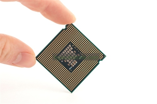
厚膜セラミック基板メーカー,Thick Film Ceramic Substrates are essential components in modern electronics, known for their robust thermal management, high mechanical strength, and excellent electrical insulation properties. Constructed from materials like alumina or aluminum nitride, these substrates support the integration of conductive, resistive, and insulating layers through a screen printing process. This technology allows precise circuit patterns to be created, enabling the development of compact, high-performance electronic devices. Widely used in power electronics, LED packaging, センサー, and automotive applications, thick film ceramic substrates ensure reliability and durability, even in harsh environments. Their ability to manage heat effectively makes them ideal for applications requiring stable performance under high temperatures.
とは Thick Film Ceramic Substrate?
A Thick Film Ceramic Substrate is a type of material used in electronics, particularly for manufacturing hybrid integrated circuits (ICの) and electronic circuits. It consists of a ceramic base onto which various layers of conductive, resistive, and insulating materials are applied using a screen printing process.
The ceramic substrate itself provides mechanical support, サーマルマネジメント, and electrical insulation for the circuit components. The thick film layers applied on top typically include conductive traces made of metals like silver, resistors made of ceramic pastes mixed with metal oxides, and insulating layers to separate different circuit elements.
These substrates are favored for their ability to handle high temperatures, making them suitable for applications where thermal management is critical. They are used in a wide range of electronic devices including sensors, パワーモジュール, LED packages, and more.
Thick Film Ceramic Substrates offer several advantages over other materials, such as high reliability, 優れた熱伝導率, and the capability to integrate multiple components into a compact space. Their robust nature makes them well-suited for harsh environments and demanding applications in industries like automotive, 航宇, および電気通信.

厚膜セラミック基板メーカー
は何ですか Thick Film Ceramic Substrate デザインガイドライン?
の設計ガイドライン thick film ceramic substrates are essential to ensure the optimal performance and reliability of electronic circuits. ここでは、いくつかの主要なガイドラインを示します:
- 材料の選択:Choose ceramic materials that have suitable thermal conductivity, 熱膨張係数 (CTEの) matching with components, と機械的強度. Common ceramics used include alumina (Al2O3) および窒化アルミニウム (AlNの).
- Layer Design: Plan the layout of conductive traces, 抵抗器, and insulating layers carefully to minimize signal interference, optimize thermal management, and ensure proper electrical isolation. Consider the placement of vias for interconnecting different layers.
- コンポーネントの配置: Position components to minimize thermal gradients and ensure uniform heating or cooling across the substrate. This is crucial for maintaining reliability and performance over the operational temperature range.
- Heat Dissipation: Incorporate thermal vias and heat sinks as necessary to dissipate heat efficiently from power components and areas of high power density. Thermal management is critical to prevent overheating and ensure long-term reliability.
- シグナルインテグリティ: Maintain signal integrity by minimizing parasitic capacitance and inductance, reducing signal crosstalk, and optimizing the impedance of signal traces. Proper grounding and shielding techniques should also be employed.
- 製造可能性: Design with manufacturability in mind, considering the capabilities of the screen printing process for thick film deposition and subsequent firing cycles. Ensure adequate spacing between features to prevent printing defects and ensure consistent layer thickness.
- 環境への配慮: Account for the operating environment of the device. Ensure the substrate and materials used can withstand temperature extremes, 湿度, 振動, and other environmental factors encountered in the application.
- 信頼性試験: Conduct thorough reliability testing to validate the design. This may include thermal cycling, humidity testing, mechanical shock, and other stress tests to ensure the substrate can withstand the expected conditions without degradation.
- ドキュメンテーション: Document the design thoroughly, including material specifications, layer configurations, component placements, and any design rules or constraints. This helps ensure consistency in manufacturing and facilitates troubleshooting and future design iterations.
これらの設計ガイドラインに従う, engineers can optimize the performance, 確実, and manufacturability of thick film ceramic substrates for various electronic applications. Each guideline plays a crucial role in ensuring the substrate meets the stringent requirements of modern electronic devices.
の利点 Thick Film Ceramic Substrate
Thick Film Ceramic Substrates offer several advantages that make them highly suitable for various electronic applications:
- サーマルマネジメント: Ceramic substrates have excellent thermal conductivity properties, 電子部品から発生する熱を効率よく放散することができます. This capability is crucial for maintaining device reliability and performance, 特にハイパワーアプリケーションの場合.
- 機械的強度: Ceramic materials, such as alumina (Al2O3) および窒化アルミニウム (AlNの), provide robust mechanical support for electronic components. They can withstand mechanical stresses and vibrations encountered in industrial and automotive environments, enhancing overall durability.
- 電気絶縁性: Ceramic substrates offer excellent electrical insulation properties, crucial for preventing electrical leakage and ensuring reliable operation of electronic circuits. This insulation capability is essential in high-voltage applications and environments where electrical noise must be minimized.
- 小型化:Thick film technology allows for the integration of multiple circuit components into a compact space on the ceramic substrate. This miniaturization capability is beneficial for reducing the overall size and weight of electronic devices while maintaining functionality.
- 設計の柔軟性: The screen printing process used in thick film technology enables flexible design options for circuit layout. Engineers can easily customize the placement of conductive traces, 抵抗器, and other components on the substrate, optimizing performance and functionality.
- コスト効率: Ceramic substrates offer cost advantages compared to other materials like PCBs (Printed Circuit Boards) for certain applications. The ability to integrate multiple functions on a single substrate and the reliability of thick film materials contribute to overall cost savings in manufacturing and operation.
- Compatibility:Ceramic substrates are compatible with a wide range of electronic components, including semiconductor devices, センサー, 抵抗器, and capacitors. This compatibility facilitates the integration of complex electronic systems on a single substrate, streamlining assembly and reducing system complexity.
- Environmental Resistance: Ceramic materials exhibit high resistance to corrosion, 湿気, および化学物質への曝露, making them suitable for harsh environmental conditions. This resistance enhances the reliability and longevity of electronic devices operating in challenging industrial, 自動車, and aerospace environments.
全, Thick Film Ceramic Substrates offer a compelling combination of thermal management, 機械的強度, 電気絶縁性, design flexibility, and cost efficiency, making them an ideal choice for a variety of electronic applications where reliability and performance are paramount.
は何ですか Thick Film Ceramic Substrate 製作プロセス?
The fabrication process of thick film ceramic substrates involves several steps to create a robust platform for electronic circuits. ここでは、一般的なプロセスの概要を示します:
- Substrate Preparation: The process begins with selecting a suitable ceramic substrate material, often alumina (Al2O3) または窒化アルミニウム (AlNの), 熱伝導率に基づく, 機械的強度, and electrical properties required for the application. The substrate is cleaned thoroughly to remove any contaminants that could affect adhesion and performance.
- Paste Formulation: Thick film pastes are formulated based on the desired properties of conductive traces, 抵抗器, and insulating layers. These pastes consist of finely ground ceramic materials mixed with binders, solvents, and additives. The composition of each paste is tailored to achieve specific electrical, メカニカル, and thermal characteristics.
- スクリーン印刷: Screen printing is the primary technique used to deposit thick film layers onto the ceramic substrate. A stencil (screen) with openings corresponding to the desired circuit pattern is placed over the substrate, and the thick film paste is forced through the openings using a squeegee. This process transfers the paste onto the substrate in the desired pattern, forming conductive traces, 抵抗器, and insulating layers.
- Drying: After screen printing, the substrate is dried to remove the solvent from the thick film paste. This step is crucial to prevent defects such as cracking or delamination during subsequent processing.
- 発射 (焼結): The dried substrate with deposited thick film layers undergoes firing in a furnace. This step involves heating the substrate to high temperatures (typically around 850-900°C for alumina) to sinter the ceramic particles in the thick film pastes. Sintering bonds the particles together, removes organic binders, and enhances the mechanical strength and electrical properties of the thick film layers.
- Trimming and Refiring (Optional): 場合によっては, additional trimming of the thick film layers may be necessary to achieve precise dimensions and electrical characteristics. This step may be followed by a brief refiring process to optimize the properties of the thick film layers.
- メタライゼーション (Optional): After the thick film layers are fired, metallization layers (often using metals like gold, 銀, or platinum) may be deposited onto the substrate to create bond pads or contacts for external connections.
- Post-Processing: The fabricated thick film ceramic substrate undergoes inspection and testing to ensure it meets the specified electrical and mechanical requirements. This may include measuring electrical resistance, checking for continuity, and inspecting for defects such as cracks or delamination.
- Integration and Assembly: Once validated, the thick film ceramic substrate is ready for integration with semiconductor devices, passive components, and other electronic elements. This integration may involve soldering, ワイヤボンディング, or other assembly techniques depending on the application requirements.
次の手順に従います, manufacturers can produce thick film ceramic substrates that offer excellent thermal management, 機械的強度, 電気絶縁性, and design flexibility for a wide range of electronic applications.
セラミックの応用 Thick Film Ceramic Substrate
Thick Film Ceramic Substrates find extensive application across various industries and electronic devices due to their excellent thermal management, 機械的強度, および電気絶縁特性. 主なアプリケーションは次のとおりです:
- パワーエレクトロニクス: Thick film ceramic substrates are commonly used in power modules and power supplies where efficient thermal dissipation is critical. They provide a robust platform for mounting power semiconductor devices like MOSFETs, IGBT関連, and diodes, helping to manage heat generation and improve reliability.
- LED Packaging: LED (発光ダイオード) modules often utilize thick film ceramic substrates due to their ability to handle high temperatures and provide effective thermal management for LEDs. These substrates help in dissipating heat generated by LEDs, ensuring prolonged operational life and consistent performance.
- Sensor Technology: Ceramic substrates are ideal for housing and interconnecting sensor elements such as temperature sensors, pressure sensors, and gas sensors. Their excellent thermal conductivity ensures accurate sensor readings, while their mechanical strength and durability make them suitable for harsh environments.
- カーエレクトロニクス: Thick film ceramic substrates are widely employed in automotive electronics for applications such as engine control units (ECU(エキュエート), transmission control modules, and power management systems. They withstand the mechanical stresses and temperature fluctuations typical of automotive environments.
- 電気通信: 通信機器, ceramic substrates are used in RF (無線周波数) modules, アンテナ, とフィルター. They provide stable electrical properties, low signal loss, と高周波性能, crucial for reliable communication systems.
- 医療機器: Ceramic substrates are used in medical devices and equipment where reliability, biocompatibility, and sterilization resistance are essential. アプリケーションには埋め込み型医療機器が含まれます, 診断機器, and surgical instruments.
- 産業用電子機器: Thick film ceramic substrates are employed in industrial automation, 制御システム, and power converters. They offer robustness against environmental factors like temperature extremes, 湿気, および化学物質への曝露, making them suitable for industrial applications.
- 家電: Ceramic substrates are found in consumer electronics such as smart appliances, ウェアラブルデバイス, and portable electronics. コンパクトなサイズ, thermal efficiency, and electrical insulation properties contribute to the miniaturization and reliability of consumer electronic products.
全, 汎用性, 耐久性, and performance characteristics of thick film ceramic substrates make them indispensable in a wide range of electronic applications across industries, contributing to advancements in technology and reliability of electronic devices.
に関するFAQ Thick Film Ceramic Substrate
What is a thick film ceramic substrate?
A thick film ceramic substrate is a type of material used in electronics, typically made of ceramic (such as alumina or aluminum nitride), onto which multiple layers of conductive, resistive, and insulating materials are applied using a screen printing process. These substrates provide mechanical support, サーマルマネジメント, and electrical insulation for electronic components.
What are the advantages of using thick film ceramic substrates?
Thick film ceramic substrates offer advantages such as excellent thermal conductivity, robust mechanical strength, 高い電気絶縁性, design flexibility for complex circuit layouts, cost-effectiveness in certain applications, and compatibility with various electronic components. These properties make them suitable for applications requiring reliability, サーマルマネジメント, and compact designs.
Where are thick film ceramic substrates used?
Thick film ceramic substrates find application in a wide range of industries and electronic devices. Common uses include power electronics (パワーモジュール, コンバーター), LED packaging, センサー (temperature, 圧力), 自動車用電子機器 (ECU(エキュエート, センサー), 電気通信 (RFモジュール, アンテナ), 医療機器, 産業用電子機器 (automation, 制御システム), および家庭用電化製品.
How are thick film ceramic substrates fabricated?
The fabrication process involves selecting a ceramic substrate material, preparing thick film pastes (conductive, resistive, insulating), screen printing these pastes onto the substrate to create circuit patterns, drying the printed layers, and firing (焼結) the substrate at high temperatures to bond the materials and enhance their properties. Optional steps may include metallization for contact pads and post-processing testing for quality assurance.
What are the key considerations when designing with thick film ceramic substrates?
Design considerations include selecting appropriate ceramic material based on thermal and mechanical requirements, optimizing layer thickness and pattern layout for thermal management and electrical performance, ensuring compatibility with electronic components, and considering environmental factors and reliability testing to meet application-specific needs.
What are the challenges associated with thick film ceramic substrates?
Challenges may include achieving precise layer thickness during screen printing, controlling shrinkage and warping during firing, managing thermal expansion mismatches with electronic components, and ensuring consistent quality across production batches. Designing for manufacturability and addressing any compatibility issues with assembly processes are also considerations.
How do thick film ceramic substrates compare to other substrate materials?
Compared to materials like printed circuit boards (プリント基板), thick film ceramic substrates offer superior thermal management capabilities, higher mechanical strength, and better electrical insulation. They are particularly advantageous in high-temperature environments and applications requiring compact designs with integrated components.
What are some specific applications where thick film ceramic substrates excel?
Specific applications include power electronics (due to thermal conductivity and mechanical robustness), LEDモジュール (for heat dissipation), 自動車用電子機器 (for durability and reliability in harsh conditions), および医療機器 (for biocompatibility and reliability). They are also prevalent in telecommunications for RF components and in industrial settings for automation and control systems.
 基板メーカー")
) セラミック基板メーカー")
) セラミック基板メーカー")
 セラミック基板メーカー")
 セラミック基板メーカー")


