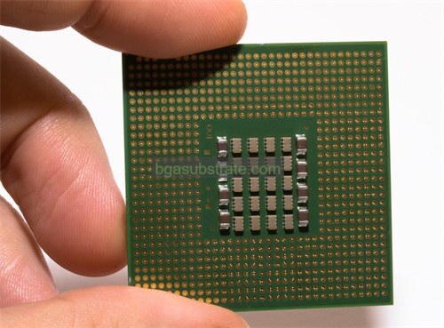
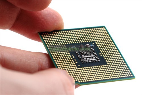
メグトロン 7 基板 生産者
メグトロン 7 基板メーカー,メグトロン 7 Substrate is an advanced material engineered for high-frequency and high-speed digital applications, renowned for its exceptional performance and reliability. It features an ultra-low dielectric constant and low dissipation factor, ensuring minimal signal loss and superior signal integrity even at high frequencies. メグトロン 7 offers outstanding thermal conductivity and stability, crucial for efficient heat dissipation and consistent electrical performance in challenging environments. Its robust mechanical properties, including high glass transition temperature and low thermal expansion, support intricate circuit designs with precision and durability. Engineers rely on Megtron 7 Substrate for critical applications in telecommunications, コンピューティング, および航空宇宙産業, 信頼性とパフォーマンスが最優先される場所.
メグトロンとは 7 基板?
メグトロン 7 substrate is an advanced material used primarily in high-frequency applications within PCB (Printed Circuit Board) manufacturing. It belongs to the Megtron series developed by Panasonic, known for their high performance and reliability in demanding electronic designs. メグトロン 7 is specifically designed to offer enhanced electrical properties, 熱安定性, and signal integrity, making it suitable for use in high-speed digital and RF (無線周波数) circuits.
Key features of Megtron 7 include its low dielectric constant (εr) and low dissipation factor (Dfの), which help minimize signal loss and maintain signal integrity at higher frequencies. This substrate also exhibits excellent thermal conductivity, aiding in the efficient dissipation of heat generated during operation, thus contributing to overall reliability and performance.
Manufactured using advanced materials and processes, メグトロン 7 PCBs are capable of supporting complex designs and meeting stringent performance requirements. They are often used in telecommunications equipment, 航空宇宙システム, high-speed computing devices, and other applications where high reliability and performance under challenging conditions are essential.
まとめ, メグトロン 7 substrate stands out for its high-frequency capabilities, 優れた電気的特性, and thermal management features, making it a preferred choice for demanding electronic applications that require reliable and high-performance PCB solutions.

メグトロン 7 基板メーカー
メグトロンとは 7 基板設計ガイドライン?
の設計ガイドライン メグトロン 7 基板 focus on optimizing the performance and reliability of PCB designs using this advanced material. Here are some key aspects typically covered in Megtron 7 substrate design guidelines:
- 材料特性: Understanding the specific electrical characteristics such as dielectric constant (εr), dissipation factor (Dfの), 熱伝導率, and coefficient of thermal expansion (CTEの). これらのプロパティは、シグナルインテグリティに影響します, サーマルマネジメント, and mechanical reliability of the PCB.
- レイヤースタックアップ: Recommended layer stackup configurations that maximize signal integrity and minimize interference between layers. This includes considerations for signal, 地面, and power planes, and the use of controlled impedance traces.
- Trace Routing: Guidelines for routing high-speed signal traces to minimize signal loss, クロストーク, and electromagnetic interference (EMIの). Techniques may include maintaining consistent trace widths, proper spacing, 鋭い角を避ける.
- Via Design: Recommendations for via structures including via types (plated-through vias, microvias), アスペクト比, and placement to ensure reliable electrical connections and thermal management throughout the PCB.
- サーマルマネジメント: Strategies for managing heat dissipation effectively across the PCB, considering the high thermal conductivity of Megtron 7. This may involve thermal vias, placement of heat-generating components, and thermal relief patterns in the copper layers.
- 機械的な考慮事項: Guidelines for designing PCBs that meet mechanical requirements such as board bending, warping, と機械的強度. This includes specifying minimum trace-to-edge distances and ensuring adequate clearance for mounting holes and component placement.
- Manufacturing and Assembly: Recommendations for PCB fabrication and assembly processes that are compatible with Megtron 7 material properties. This includes soldering temperatures, compatibility with surface finishes, and handling precautions to prevent damage during manufacturing.
- Reliability and Testing: Guidelines for reliability testing and verification methods specific to PCBs using Megtron 7 基板. This ensures that the final design meets performance specifications under anticipated operational conditions.
これらの設計ガイドラインに従うことにより、, engineers can leverage the unique properties of Megtron 7 substrate to design PCBs that deliver high performance, 確実, and longevity in applications requiring advanced electrical and thermal management capabilities.
Megtronの利点 7 基板
メグトロン 7 基板 offers several advantages that make it highly desirable for advanced PCB applications:
- 高周波性能: メグトロン 7 has a low dielectric constant (εr) and low dissipation factor (Dfの), which enable excellent signal integrity at high frequencies. This property is crucial for applications requiring high-speed data transmission and RF circuits.
- Excellent Thermal Conductivity: The substrate exhibits high thermal conductivity compared to traditional PCB materials. This property helps in efficient heat dissipation from heat-generating components, enhancing overall reliability and longevity of the PCB.
- Mechanical Strength and Reliability: メグトロン 7 has good mechanical properties, including high dimensional stability and resistance to mechanical stress. This makes it suitable for applications where PCBs may undergo mechanical strain or need to withstand harsh environmental conditions.
- 環境サステナビリティ: It meets environmental regulations such as RoHS (Restriction of Hazardous Substances), ensuring that PCBs made with Megtron 7 are environmentally friendly and safe for use in various electronic devices.
- Compatibility with Advanced Manufacturing Processes: メグトロン 7 is compatible with advanced PCB manufacturing techniques such as microvia technology, which allows for higher density interconnections and miniaturization of electronic devices.
- Reliability in High-Temperature Environments: It exhibits stability and performance consistency even at elevated temperatures, making it suitable for applications that operate in demanding thermal conditions.
- コスト効率: While considered a premium material, the performance benefits of Megtron 7 often justify its cost in applications requiring high reliability and performance.
全, メグトロン 7 substrate offers a balanced combination of electrical performance, 熱管理機能, 機械的な堅牢性, and environmental compliance, making it a preferred choice for complex and high-performance PCB designs in sectors such as telecommunications, 航宇, and high-speed computing.
メグトロンとは 7 基板製造プロセス?
Megtronの製造プロセス 7 substrate involves several steps to ensure the material’s properties are preserved and optimized for high-performance PCB applications. ここでは、一般的な製造プロセスの概要を示します:
- 材料の選択:メグトロン 7 substrate starts with selecting the appropriate laminate materials that meet the desired specifications for dielectric constant (εr), dissipation factor (Dfの), 熱伝導率, および機械的特性. These materials are typically epoxy resin-based with glass fiber reinforcement.
- Prepreg Preparation: Prepregs are resin-impregnated fiberglass sheets that are cut and prepared according to the required thickness and layer stackup configuration for the PCB design.
- 錬成: After layer stackup preparation, the PCB panels are drilled with precision to create holes for vias and component mounting. Advanced drilling techniques may be used to achieve high-density interconnects (HDIs) and microvias.
- 銅箔ラミネート: Copper foil sheets are laminated onto both sides of the prepreg layers using heat and pressure. This forms the conductive layers (traces, パッド, and planes) of the PCB.
- エッチング: A chemical etching process is employed to remove excess copper from the PCB surface, leaving behind the desired circuit traces and patterns as per the PCB design.
- Plating and Surface Finish: Copper-plating processes are used to metallize the walls of the drilled holes, forming vias that establish electrical connections between different layers. Surface finishes such as immersion gold, ハスレ (熱風はんだレベリング), または OSP (Organic Solderability Preservatives) are applied to protect exposed copper and facilitate soldering during assembly.
- ソルダーマスクアプリケーション: A solder mask layer is applied over the PCB surface, leaving openings (exposed pads) for soldering component leads and connections.
- Silkscreen Printing: Identifying markings, component outlines, and other information are printed onto the PCB surface using a silkscreen printing process.
- テストと検査: Quality control processes including electrical testing, dimensional inspection, and automated optical inspection (AOI) are performed to ensure the PCB meets design specifications and reliability standards.
- Final Fabrication Steps: After testing and inspection, the PCB panels are routed or scored to separate individual boards. Edge plating or other edge treatments may be applied as necessary.
- 最終検査と梱包: Each PCB undergoes final inspection to verify functionality and quality. They are then packed and prepared for shipment to the end-user or assembly facility.
製造プロセス全体を通して, strict adherence to design guidelines and manufacturing best practices ensures that Megtron 7 substrate retains its high-frequency performance, 熱伝導率, 機械的強度, と信頼性, 要求の厳しい電子アプリケーションに適しています.
セラミックメグトロンの応用 7 基板
メグトロン 7, despite its name suggesting a ceramic substrate, is actually a high-performance epoxy-based material used primarily in printed circuit boards (プリント基板) rather than in ceramic applications. Here’s how Megtron 7 substrate is typically applied in PCBs:
- 高周波プリント基板: メグトロン 7 is widely used in high-frequency PCB applications where signal integrity is critical. Its low dielectric constant (εr) and low dissipation factor (Dfの) help minimize signal loss and maintain high-speed data transmission capabilities. This makes it suitable for telecommunications equipment, high-speed computing devices, and RF (無線周波数) アプリケーション.
- サーマルマネジメント: Due to its high thermal conductivity, メグトロン 7 is effective in dissipating heat generated by components on the PCB. This property is beneficial in electronic devices where thermal management is crucial to maintaining optimal performance and reliability.
- 機械的安定性: メグトロン 7 exhibits good dimensional stability and mechanical strength, making it suitable for PCBs that may be subjected to mechanical stress or environmental factors. This includes applications in aerospace, 自動車用電子機器, and industrial control systems.
- Miniaturization and HDI: メグトロン 7 supports advanced PCB manufacturing techniques such as microvia technology and high-density interconnects (HDIの). These capabilities allow for miniaturization of electronic devices and the integration of complex circuit designs.
- Reliability in Harsh Environments: Its stability and performance consistency at elevated temperatures make Megtron 7 suitable for use in applications exposed to harsh operating conditions, such as military electronics and outdoor telecommunications equipment.
まとめ, メグトロン 7 substrate is primarily used in PCBs where high-frequency performance, 優れた熱管理, 機械的な堅牢性, and reliability are critical requirements. It enables the development of advanced electronic devices that demand superior electrical properties and operational efficiency.
Megtronについてよくある質問 7 基板
What are the key advantages of using Megtron 7 基板?
メグトロン 7 offers advantages such as low dielectric constant (εr) and low dissipation factor (Dfの) for high-speed signal integrity, 効果的な熱放散のための高い熱伝導率, and mechanical strength for durability in challenging environments.
In what applications is Megtron 7 substrate commonly used?
It is used in high-frequency PCBs, 通信機器, RF applications, 航空宇宙エレクトロニクス, 自動車用電子機器, and other devices requiring reliable performance under demanding conditions.
What are the fabrication processes involved in making PCBs with Megtron 7 基板?
The fabrication process includes material selection, prepreg preparation, 錬成, 銅箔ラミネート, エッチング, 鍍金, 表面仕上げ, ソルダーマスクアプリケーション, silkscreen printing, テスティング, 検査, そして最終的な包装.
メグトロンはどうですか 7 substrate compare to other PCB materials like FR4?
Compared to FR4, メグトロン 7 offers superior high-frequency performance, better thermal conductivity, and enhanced mechanical stability, making it suitable for applications where these properties are critical.
Is Megtron 7 substrate environmentally friendly?
はい, メグトロン 7 substrate complies with environmental regulations such as RoHS (Restriction of Hazardous Substances), ensuring it is safe for use in electronic devices.
What are the considerations when designing PCBs with Megtron 7 基板?
Design considerations include optimizing layer stackup for signal integrity, managing thermal dissipation effectively, using appropriate via designs, and ensuring compatibility with manufacturing processes that support advanced PCB technologies.
Where can Megtron 7 substrate be sourced?
メグトロン 7 substrate is typically available through PCB material suppliers and manufacturers that specialize in high-performance electronic materials.
 あなたのウェブサイト名

