
BGA/IC Substrate Fabricant
Fabricant de substrats BGA/IC,BGA (Grille à billes) and IC (Integrated Circuit) substrates are essential components in semiconductor packaging, providing a foundation for mounting and interconnecting microchips. BGA substrates feature an array of solder balls on the underside, allowing for reliable and high-density connections between the chip and the printed circuit board (PCB). IC substrates, including those used for BGA packages, offer excellent electrical insulation, Gestion thermique, and mechanical support. They are designed to accommodate high pin counts and support high-speed data transmission. These substrates are widely used in various electronic devices, including processors, memory modules, and communication systems, enabling compact and efficient designs.
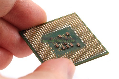
Quoi BGA/IC Substrate?
A BGA (Grille à billes) substrat, also known as an IC (Integrated Circuit) substrat, is a type of printed circuit board (PCB) specifically designed to support the mounting and interconnection of ball grid array packages. These substrates are crucial in the electronics industry, serving as the foundational layer where ICs are soldered and connected to the rest of the circuit.
BGA substrates typically consist of multiple layers of conductive and insulating materials. The primary function of these substrates is to provide a reliable electrical connection between the IC’s balls (solder balls) and the PCB. This is achieved through a network of fine-pitch copper traces and vias that facilitate the electrical pathways between the IC and the external components.
Key characteristics of BGA substrates include their ability to support high-density interconnections and high-frequency signals. They are designed to handle the thermal and mechanical stresses associated with IC packages, ensuring long-term reliability and performance. The substrates are also engineered to manage heat dissipation effectively, which is critical for preventing overheating and maintaining the stability of the electronic system.
In addition to their primary role in electronic assemblies, BGA substrates are integral to advanced applications such as high-speed computing, télécommunication, et l’électronique grand public. Their design and fabrication involve precise engineering to meet stringent requirements for signal integrity, Gestion thermique, and mechanical robustness.

Fabricant de substrats BGA/IC
Qu’est-ce que le BGA/IC Substrate Directives de conception?
Conception BGA (Grille à billes) and IC (Integrated Circuit) substrates involves careful consideration of various factors to ensure optimal performance, fiabilité, et fabricabilité. Here are key design guidelines for BGA and IC substrates:
- Sélection des matériaux: Choose appropriate substrate materials based on the application’s requirements. High-performance materials such as FR4, BT resin, ceramics, and high-density organic materials should be selected for their thermal, mécanique, et propriétés électriques.
- Empilement de couches: Design the substrate with an appropriate layer stackup to balance signal integrity, Gestion thermique, et stabilité mécanique. Multi-layer designs are often used to accommodate complex routing and minimize signal interference.
- Pad and Via Design: Ensure proper pad and via dimensions to match the BGA or IC package specifications. Adequate pad sizes and via placements are crucial for reliable solder joint formation and electrical connectivity.
- Gestion thermique: Incorporate thermal vias, heat sinks, and other thermal management techniques to dissipate heat generated by the ICs. Effective thermal management prevents overheating and ensures stable performance.
- Intégrité du signal: Design signal traces to minimize noise and interference. Use controlled impedance routing for high-speed signals and ensure proper grounding to reduce electromagnetic interference (EMI).
- Mechanical Considerations: Ensure the substrate’s mechanical design can handle the stress and strain during assembly and operation. Consider factors such as substrate warpage and mechanical strength.
- Fabricabilité: Concevoir le substrat pour qu’il soit compatible avec les processus de fabrication standard. Avoid overly complex designs that could lead to manufacturing challenges or increased costs.
- Essais et inspections: Incorporate test points and design for manufacturability (DFM) practices to facilitate testing and inspection. This helps in identifying potential issues early in the production process.
- Reliability and Robustness: Design the substrate to withstand environmental conditions such as temperature extremes, humidité, et contraintes mécaniques. Ensure that the substrate meets reliability standards and passes rigorous testing.
- Compliance and Standards: Follow industry standards and guidelines, such as IPC-2221 for PCB design and IPC-7351 for land pattern design, to ensure compatibility and reliability.
En respectant ces directives, designers can create BGA and IC substrates that offer high performance, fiabilité, and ease of manufacturability, meeting the demands of modern electronic systems.
Les avantages de BGA/IC Substrate
BGA (Grille à billes) and IC (Integrated Circuit) substrates offer several significant advantages in electronic packaging and circuit design. Voici les principaux avantages:
- Higher Pin Density: BGA substrates allow for a higher pin density compared to traditional package types like DIP (Dual In-line Package) and QFP (Quad Flat Package). This enables the design of more compact and densely packed circuits, which is essential for modern electronic devices.
- Amélioration des performances électriques: The BGA design reduces signal path lengths and provides better signal integrity due to shorter and more direct connections between the IC and the PCB. This results in enhanced electrical performance, including reduced signal degradation and lower impedance.
- Gestion thermique améliorée: BGA substrates often incorporate features like thermal vias and heat spreaders to improve heat dissipation. This is particularly important for high-power ICs, as it helps prevent overheating and ensures stable operation.
- Reduced Package Size: The BGA package design enables smaller and more compact PCB layouts. This is beneficial for portable and space-constrained applications where minimizing the overall size of the electronic device is crucial.
- Improved Mechanical Reliability: The BGA’s solder ball grid design provides more robust mechanical connections compared to traditional pin-based packages. This design helps to absorb mechanical stresses and reduce the risk of solder joint failure.
- Better Alignment and Assembly: The BGA package’s grid of solder balls simplifies the alignment process during assembly and enhances the reliability of soldering. Automated placement and soldering processes are more straightforward with BGA packages.
- Réduction des interférences électromagnétiques (EMI): The BGA design often includes better shielding and grounding techniques, which help in reducing electromagnetic interference. This is particularly important for high-frequency applications.
- Évolutivité: BGA and IC substrates are highly scalable and can accommodate a wide range of package sizes and types. This flexibility allows for easy integration into various electronic devices and systems.
- Cost-Effective Production: While the initial setup costs for BGA and IC substrates may be higher, their design often leads to cost savings in manufacturing and assembly due to improved automation and reduced assembly time.
- Durabilité accrue: BGA substrates typically offer better resistance to mechanical stresses and thermal cycling, which contributes to the overall durability and reliability of the electronic device.
En résumé, BGA and IC substrates provide numerous advantages, including higher pin density, Amélioration des performances électriques et thermiques, reduced package size, et fiabilité accrue. These benefits make them well-suited for modern electronic devices and applications.
Qu’est-ce que le BGA/IC Substrate Processus de fabrication?
The fabrication of BGA (Grille à billes) and IC (Integrated Circuit) substrates involves several intricate steps to ensure high performance and reliability. Voici un aperçu du processus de fabrication typique:
- Sélection des matériaux: The process begins with the selection of suitable substrate materials, such as FR4, BT resin, ceramics, or high-density organic materials. These materials are chosen based on their electrical, thermique, and mechanical properties.
- Laminage: Layers of substrate material are laminated together to form a multi-layered structure. This step involves applying heat and pressure to bond the layers, creating a solid base for further processing.
- Photolithographie: A photosensitive coating (photoresist) is applied to the surface of the substrate. The substrate is then exposed to ultraviolet (UV) light through a mask that defines the circuit patterns. The exposed photoresist is developed, leaving behind a pattern for subsequent etching.
- Gravure: The exposed areas of the substrate are etched away using chemical solutions or plasma etching, laissant derrière soi les modèles de circuit souhaités. This process creates the traces, Tampons, and vias required for electrical connectivity.
- Placage: Metal layers, typically copper, are deposited onto the substrate through electroplating or electroless plating. This metal deposition forms the conductive paths necessary for electrical connections.
- Drilling and Via Formation: Holes (Vias) are drilled into the substrate to create connections between different layers of the multi-layer structure. These vias are then plated with metal to ensure electrical continuity.
- Application du masque de soudure: A solder mask layer is applied over the substrate, except for the areas where soldering will occur. This layer protects the circuit from accidental solder bridging and contamination during the assembly process.
- Finition de surface: A surface finish, such as HASL (Nivellement de la soudure à l’air chaud), ENIG (Nickel autocatalytique par immersion d’or), ou OSP (Conservateur de soudabilité organique), is applied to the exposed metal surfaces to improve solderability and protect against oxidation.
- BGA Ball Attachment: For BGA substrates, solder balls are attached to the designated areas on the underside of the substrate. This is typically done using a reflow soldering process, where solder paste is applied, and then solder balls are placed and melted to form a grid pattern.
- Inspection et essais: The fabricated substrate undergoes rigorous inspection and testing to ensure quality and reliability. Cela inclut l’inspection visuelle, Essais électriques, and functional testing to identify any defects or issues.
- Cutting and Shaping: The substrates are cut and shaped to the required dimensions and specifications. This step may involve separating individual substrate panels or trimming to final package sizes.
- Assemblage final: The substrates are then assembled into their final packages, which may include attaching ICs or other components, and undergoing final testing to ensure proper functionality and performance.
En résumé, the BGA/IC substrate fabrication process involves multiple steps, including material selection, laminage, photolithographie, gravure, Placage, forage, Application du masque de soudure, finition de surface, ball attachment, inspection, et l’assemblage final. Each step is crucial to ensuring that the substrate meets the required performance and reliability standards.
L’application de la céramique BGA/IC Substrate
Ceramic BGA (Grille à billes) and IC (Integrated Circuit) substrates are used in a variety of high-performance and specialized electronic applications. Here are some key applications of ceramic BGA/IC substrates:
- High-Frequency and High-Speed Electronics: Ceramic substrates are ideal for high-frequency and high-speed electronic applications due to their excellent electrical performance and low signal loss. They are used in RF (Radiofréquence) et circuits micro-ondes, where signal integrity and minimal loss are critical.
- Electronique de puissance:Ceramic substrates are commonly used in power electronics, including power converters, Onduleurs, and power amplifiers. Their superior thermal conductivity and thermal management properties help dissipate heat efficiently, which is essential for high-power applications.
- Électronique automobile: Dans l’industrie automobile, ceramic substrates are used in critical applications such as engine control units (Écus), advanced driver-assistance systems (ADAS), and ignition systems. Their robustness and reliability make them suitable for harsh automotive environments.
- Aérospatiale et défense: Ceramic substrates are employed in aerospace and defense applications due to their high reliability and ability to withstand extreme environmental conditions. They are used in satellite communications, avionique, and military electronics where performance and durability are paramount.
- Dispositifs médicaux: In the medical field, ceramic BGA/IC substrates are used in various high-precision and reliability-demanding devices such as imaging systems, Équipement de diagnostic, et dispositifs implantables. Their biocompatibility and performance under extreme conditions are critical for medical applications.
- Électronique grand public: Ceramic substrates are also used in high-end consumer electronics, including smartphones, Comprimés, et consoles de jeux. They provide enhanced performance and miniaturization benefits, which are essential for modern electronic devices.
- Communication Infrastructure: Ceramic substrates are used in communication infrastructure components such as base stations, Antennes, and high-speed data transceivers. Their ability to handle high frequencies and high power levels makes them suitable for telecommunications applications.
- Optoelectronics: In optoelectronic devices, such as laser diodes and light-emitting diodes (Led), ceramic substrates are used to provide stable performance and efficient thermal management. They help ensure the longevity and reliability of optoelectronic components.
- High-Reliability Applications: Ceramic substrates are chosen for high-reliability applications where failure is not an option. This includes critical systems in various industries where durability, Gestion thermique, and electrical performance are essential.
- Power Modules: In power modules, ceramic substrates are used to support and interconnect power semiconductor devices. Their high thermal conductivity and electrical insulation properties are crucial for the efficient operation and longevity of power modules.
En résumé, ceramic BGA and IC substrates are utilized in diverse applications where high performance, fiabilité, and durability are required. Their superior electrical, thermique, and mechanical properties make them suitable for demanding environments and advanced electronic systems.
FAQ sur BGA/IC Substrate
What is a BGA substrate?
A BGA (Grille à billes) substrate is a type of printed circuit board (PCB) that supports BGA packages. It features a grid of solder balls on its underside that connects the package to the PCB, allowing for higher pin density and compact designs.
What is an IC substrate?
An IC (Integrated Circuit) substrate is a material platform that supports and interconnects IC chips. It provides mechanical support, electrical connections, and thermal management for the integrated circuits.
What materials are used in BGA/IC substrates?
Les matériaux courants incluent le FR4 (fiberglass-reinforced epoxy resin), BT resin (bismaleimide-triazine), ceramics, and high-density organic materials. The choice depends on the specific requirements of the application, such as thermal and electrical performance.
What are the benefits of using BGA substrates?
BGA substrates offer advantages such as higher pin density, Amélioration des performances électriques, reduced package size, une meilleure gestion thermique, and enhanced mechanical reliability.
How is a BGA substrate different from a standard PCB?
A BGA substrate is specifically designed to support BGA packages, featuring a grid of solder balls for connection. In contrast, a standard PCB may use other types of connections, such as through-hole or surface-mount technology.
What is the role of thermal management in BGA/IC substrates?
Thermal management ensures that heat generated by the ICs is efficiently dissipated. BGA/IC substrates may include thermal vias, heat spreaders, and other techniques to prevent overheating and maintain reliable performance.


 Fabricant de substrats céramiques")

