Embedded Cavity Substrate Hersteller
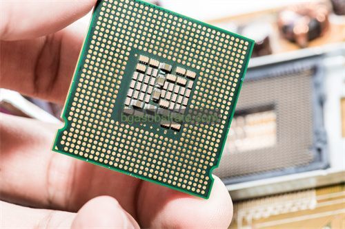
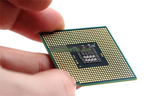
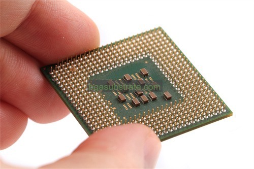
Hersteller von eingebetteten Hohlraumsubstraten,Embedded cavity substrates are advanced packaging solutions that feature cavities within the substrate material to house electronic components, such as chips or passive elements. This design enables the integration of components within the substrate itself, leading to reduced overall package size and improved electrical performance. By embedding components, these substrates provide better protection and enhance thermal management, as heat can be efficiently dissipated. Embedded cavity substrates are particularly useful in high-density, high-speed, und Hochfrequenzanwendungen, wie HF- und Mikrowellenschaltungen, where minimizing signal loss and interference is critical. They are commonly used in advanced communication systems, Sensoren, and other compact electronic devices.
Was ist Embedded Cavity Substrate?
An Embedded Cavity Substrate is a specialized type of printed circuit board (PLATINE) designed to enhance the performance of electronic devices by integrating cavities or channels within the PCB structure. These cavities are typically created through a manufacturing process that involves etching or milling away portions of the substrate to form spaces or voids.
The primary advantage of embedded cavity substrates lies in their ability to accommodate high-frequency and high-speed signals with minimal signal loss and interference. By embedding cavities, designers can achieve better impedance control and reduce the overall size of the PCB, which is particularly beneficial in compact and high-performance applications such as mobile devices, Luft- und Raumfahrt, und Automobilelektronik.
Embedded cavity substrates are commonly used in high-frequency applications because they can be tailored to specific signal requirements and offer improved thermal management. The cavities can also be used to house components or integrate additional layers of circuitry, further optimizing the PCB design.
Manufacturing embedded cavity substrates involves precise techniques to ensure that the cavities are accurately formed and aligned with the circuit traces. This process often requires advanced technology and materials to achieve the desired electrical and mechanical properties. The integration of cavities can also contribute to weight reduction and better thermal dissipation, which are critical factors in modern electronic device design.
Insgesamt, embedded cavity substrates represent a significant advancement in PCB technology, providing enhanced performance and functionality for a wide range of electronic applications.

Hersteller von eingebetteten Hohlraumsubstraten
Was ist das Embedded Cavity Substrate Richtlinien für die Gestaltung?
Embedded Cavity Substrate Design Guidelines are essential principles and practices to ensure the effective use of embedded cavity technology in PCB designs. These guidelines help optimize the performance, Zuverlässigkeit, and manufacturability of embedded cavity substrates. Here are key aspects to consider:
- Cavity Placement and Size: Determine the appropriate location and dimensions of cavities based on the components being embedded. Ensure that the cavities are strategically placed to minimize signal interference and to facilitate effective thermal management.
- Materialauswahl: Choose substrate materials with suitable thermal and electrical properties for the specific application. The materials should support the intended frequency, Signalintegrität, and thermal dissipation requirements.
- Fertigungstoleranzen: Maintain tight tolerances during the fabrication of cavities to ensure proper fit and alignment of embedded components. Accurate cavity dimensions are crucial for achieving desired performance and preventing assembly issues.
- Wärmemanagement: Design the substrate to effectively dissipate heat generated by embedded components. Consider the thermal conductivity of the substrate material and incorporate heat sinks or thermal vias if necessary.
- Signalintegrität: Minimize signal loss and interference by optimizing cavity design and layout. Ensure proper routing of signal traces and consider the effects of cavity walls on high-speed signals.
- Mechanical Support: Ensure that embedded components are adequately supported to prevent mechanical stress or damage during assembly and operation. The substrate should provide sufficient mechanical stability for the components.
- Manufacturing Process: Understand the specific requirements of the manufacturing process, including laser drilling, Radierung, and lamination. Ensure that the design is compatible with the capabilities of the fabrication equipment.
- Testen und Validieren: Implement thorough testing procedures to validate the performance and reliability of the embedded cavity substrate. This includes electrical, thermisch, and mechanical testing to ensure the design meets all requirements.
- Design für die Montage (DFA): Consider ease of assembly during the design phase. Ensure that the substrate design facilitates efficient and accurate placement of components and minimizes potential assembly challenges.
- Documentation: Provide clear and detailed design documentation, including cavity dimensions, material specifications, and assembly instructions. This ensures that all stakeholders have the necessary information for successful manufacturing and assembly.
Indem Sie diese Richtlinien befolgen, designers can effectively leverage embedded cavity technology to create compact, high-performance substrates that meet the demands of modern electronic applications.
Die Vorteile von Embedded Cavity Substrate
The Advantages of Embedded Cavity Substrate are numerous and contribute significantly to the advancement of electronic packaging and design. Hier sind einige der wichtigsten Vorteile:
- Reduced Size and Weight: By embedding components within the substrate, the overall size and weight of the electronic device are significantly reduced. This compact design is ideal for miniaturized applications where space is at a premium.
- Verbesserte Signalintegrität: Embedded cavity substrates facilitate shorter signal paths and reduce the distance between components, which minimizes signal loss and interference. This results in enhanced signal integrity and better performance, especially in high-speed and high-frequency applications.
- Verbessertes Wärmemanagement: The design of embedded cavity substrates allows for effective heat dissipation. Components embedded within the substrate benefit from improved thermal conductivity and heat spreading, which helps to manage and dissipate heat more efficiently.
- Increased Reliability: Embedding components within the substrate provides better protection against mechanical stress and environmental factors. This enhances the overall reliability and durability of the electronic device, reducing the risk of component damage and failure.
- Higher Component Density: Embedded cavity substrates enable a higher density of components within a given area, supporting the development of more complex and sophisticated electronic systems. This is particularly valuable for applications requiring dense interconnections and functionalities.
- Verbesserte elektrische Leistung: The reduction in signal path lengths and the optimization of the layout contribute to better electrical performance. This includes improved impedance control, reduced crosstalk, and enhanced overall circuit efficiency.
- Simplified Assembly: By embedding components directly within the substrate, the need for additional assembly steps, such as soldering or mounting on a separate PCB, is minimized. This can streamline the assembly process and reduce production costs.
- Enhanced Design Flexibility: The use of embedded cavities allows for more innovative and flexible design solutions. Designers can create complex and optimized layouts that are difficult to achieve with traditional surface-mount technology.
- Reduzierte elektromagnetische Störungen (EMI): The embedded design can help reduce EMI by shielding sensitive components and circuits within the substrate. This results in improved performance and reduced susceptibility to external interference.
- Kosteneffizienz: Although the initial manufacturing cost may be higher, the benefits of reduced size, weight, and assembly complexity can lead to long-term cost savings. Zusätzlich, the improved reliability can result in lower maintenance and replacement costs.
Insgesamt, embedded cavity substrates offer significant advantages in terms of size, Leistung, und Zuverlässigkeit, making them a valuable choice for advanced electronic packaging and design applications.
Was ist das Embedded Cavity Substrate Herstellungsprozess?
Embedded Cavity Substrate Fabrication Process involves several intricate steps to create substrates with embedded cavities. Here is a detailed overview of the process:
- Design und Layout: The process begins with the design phase, where engineers create detailed layouts of the substrate, including the locations, sizes, and shapes of the cavities. This design is typically developed using CAD (Computer-Aided Design) software, ensuring precision and alignment with component requirements.
- Materialauswahl: Choose appropriate substrate materials based on the desired thermal, elektrisch, und mechanische Eigenschaften. Zu den gängigen Materialien gehört FR4, high-frequency laminates, or specialized composites. The selected materials should support the intended application and fabrication process.
- Cavity Formation:The cavities are created using various techniques:
– Laser Drilling: A laser is used to precisely drill holes into the substrate material where cavities are to be formed. This technique is suitable for creating fine features and achieving high accuracy.
– Mechanical Drilling: For larger cavities, mechanical drilling or routing may be used to remove material and form the required cavity shapes.
– Chemical Etching: In einigen Fällen, chemical etching processes can be employed to create cavities by selectively removing material from the substrate.
- Schichtung: The substrate layers are laminated together using heat and pressure to bond them into a single, cohesive structure. During this step, the cavity structures are aligned with the substrate layers to ensure proper integration.
- Component Placement: Components are placed into the pre-formed cavities. This step may involve precision placement techniques to ensure accurate alignment and fitting of the components within the cavities.
- Cavity Filling (if applicable): In some designs, cavities may be filled with additional materials, such as dielectric fillers or adhesive, to secure the embedded components and enhance the structural integrity of the substrate.
- Layer Processing: Additional layers may be applied to the substrate, including circuitry, solder masks, and other functional elements. These layers are processed using standard PCB fabrication techniques such as etching, Beschichtung, and printing.
- Electrical Testing: The substrate undergoes electrical testing to ensure that all connections, signal paths, and components are functioning correctly. This testing verifies the performance and reliability of the substrate.
- Final Inspection and Quality Control: The finished substrate is inspected for quality assurance. Dazu gehört auch die Sichtprüfung, dimensional checks, and any additional tests to ensure that the substrate meets all design specifications and performance requirements.
- Montage und Verpackung: The completed embedded cavity substrate is assembled into the final electronic device or system. This may involve additional assembly steps, such as integration with other components, Verkapselung, und Endverpackung.
Indem Sie diese Schritte befolgen, manufacturers can produce embedded cavity substrates that offer improved performance, compactness, and reliability for advanced electronic applications. The complexity of the process requires precision and attention to detail to achieve high-quality results.
Die Anwendung von Keramik Embedded Cavity Substrate
The Application of Ceramic Embedded Cavity Substrate offers a range of advantages in various advanced electronic systems. Here’s an overview of how ceramic embedded cavity substrates are applied:
- High-Frequency and RF Applications: Ceramic embedded cavity substrates are widely used in high-frequency and radio frequency (RF) applications due to their excellent dielectric properties. The low dielectric loss and high thermal conductivity of ceramics make them ideal for RF circuit boards, antenna modules, and communication devices where signal integrity and minimal signal loss are crucial.
- Microwave and Millimeter-Wave Circuits: In microwave and millimeter-wave circuits, ceramic embedded cavity substrates provide superior performance. The precise cavity structures help in achieving high-Q resonators and filters, which are essential for applications in radar systems, Satellitenkommunikation, and advanced imaging systems.
- Leistungselektronik: For power electronics, ceramic substrates with embedded cavities help manage thermal dissipation effectively. They are used in high-power applications such as power amplifiers, voltage regulators, and converters. The efficient heat management capabilities of ceramics ensure reliable operation and longevity of power components.
- Medizinprodukte: In der Medizinelektronik, ceramic embedded cavity substrates are used for their biocompatibility, Zuverlässigkeit, and high performance. Applications include implantable medical devices, Diagnosegeräte, und Sensoren. The ability to miniaturize components while maintaining high performance is crucial in medical device design.
- Luft- und Raumfahrt und Verteidigung: The aerospace and defense industries benefit from ceramic embedded cavity substrates due to their ability to withstand harsh environments and high temperatures. These substrates are used in avionics, Radarsysteme, and communication devices where durability and performance under extreme conditions are essential.
- Fahrzeugelektronik: Im Automotive-Bereich, ceramic substrates are employed in advanced driver assistance systems (ADAS), Infotainment-Systeme, and control modules. Their thermal stability and reliability ensure that electronic systems perform reliably in the demanding automotive environment.
- Unterhaltungselektronik: Ceramic embedded cavity substrates are also used in high-performance consumer electronics, such as smartphones, Tabletten, and wearable devices. The ability to integrate high-density circuits and manage heat effectively helps in designing compact and efficient consumer devices.
- Industrielle Automatisierung: In industrial automation, ceramic substrates with embedded cavities are used in control systems, Sensoren, and actuators. The reliability and robustness of ceramic materials support the performance of electronic systems in industrial environments.
- Military Systems: For military applications, the high-performance characteristics of ceramic substrates are leveraged in communication systems, electronic warfare equipment, and navigation systems. The substrates offer durability, Signalintegrität, and resistance to environmental stresses.
- Wireless Charging: In wireless charging systems, ceramic embedded cavity substrates help in efficient power transfer and signal coupling. The substrate’s properties support the design of compact and efficient charging solutions.
Insgesamt, ceramic embedded cavity substrates provide significant benefits across a range of high-performance and high-reliability applications. Ihre einzigartigen Eigenschaften, including excellent thermal management, geringer dielektrischer Verlust, und mechanische Robustheit, make them suitable for demanding electronic systems.
Häufig gestellte Fragen zur Embedded Cavity Substrate
What is an embedded cavity substrate?
An embedded cavity substrate is a type of printed circuit board (PLATINE) where cavities are created within the substrate material to house and protect electronic components. This design helps to reduce the overall size, improve performance, and enhance thermal management.
What are the advantages of using embedded cavity substrates?
The advantages include reduced size and weight, Verbesserte Signalintegrität, besseres Wärmemanagement, increased reliability, higher component density, and simplified assembly.
What materials are used for embedded cavity substrates?
Zu den gängigen Materialien gehört FR4, high-frequency laminates, and ceramics. The choice of material depends on the specific application requirements such as thermal conductivity, dielectric properties, und mechanische Festigkeit.
How are cavities created in the substrate?
Cavities can be formed using laser drilling, mechanical drilling, chemical etching, or other precision techniques to remove material and create the desired shapes and sizes.
What applications use embedded cavity substrates?
They are used in high-frequency and RF applications, microwave and millimeter-wave circuits, Leistungselektronik, medizinprodukte, Luft- und Raumfahrt und Verteidigungssysteme, Fahrzeugelektronik, Unterhaltungselektronik, Industrielle Automatisierung, and wireless charging systems.
How does embedded cavity technology improve thermal management?
By embedding components within the substrate, heat is more effectively dissipated through the substrate material, which helps to manage and spread heat generated by the components.
 Name Ihrer Website

