ABF Substrate Hersteller
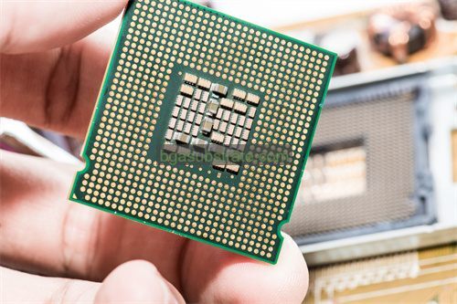
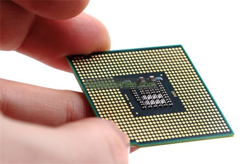
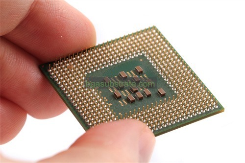
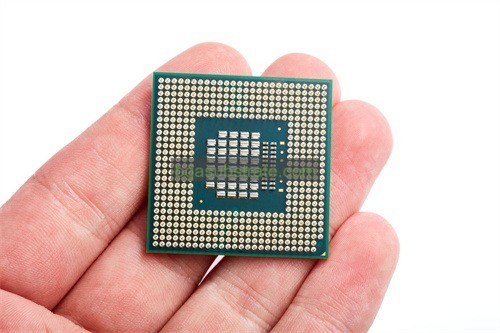
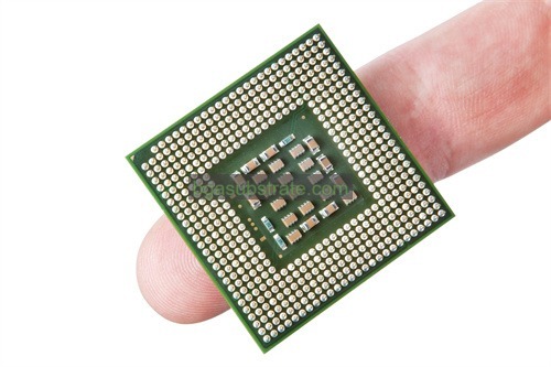
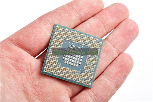
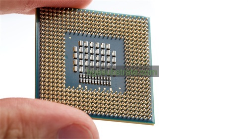
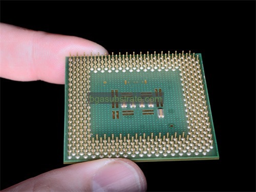
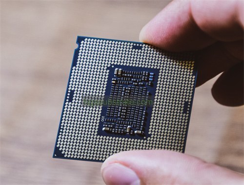
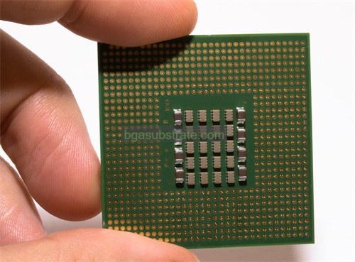
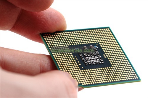
Hersteller von ABF-Substraten,ABF (Ajinomoto Build-up Film) substrates are advanced materials used in the fabrication of semiconductor packaging, particularly for high-density and high-performance applications. They are made from a unique epoxy resin system developed by Ajinomoto, which provides excellent electrical insulation, mechanische Festigkeit, and thermal stability. ABF substrates are widely used in flip chip packaging, enabling fine pitch interconnections and supporting high-speed signal transmission. Their low dielectric constant and low loss tangent make them ideal for high-frequency applications, such as CPUs, GPUs, and networking devices. ABF substrates are crucial in achieving miniaturization and enhancing the performance of modern electronic devices.
Was ist ABF Substrate?
ABF (Ajinomoto Build-up Film) substrate is a type of advanced printed circuit board (PLATINE) material developed by Ajinomoto Co., Inc. This substrate is specifically designed for high-performance electronic applications, particularly in the realm of integrated circuit (ISCH) packaging.
ABF substrates are known for their superior electrical and thermal properties, which make them suitable for high-density interconnect (HDI) anträge. They offer excellent performance in terms of dielectric constant and low dissipation factor, which are crucial for high-speed and high-frequency signal transmission. The film’s build-up structure enables the creation of multiple layers of circuitry, allowing for compact and complex circuit designs with improved reliability and performance.
One of the main advantages of ABF substrates is their ability to handle finer line and space requirements compared to traditional PCB materials. This is due to their low thermal expansion coefficient and excellent bonding characteristics, which contribute to the overall durability and stability of the IC package. Zusätzlich, ABF substrates facilitate the manufacturing of advanced flip-chip packages, which are widely used in modern electronic devices due to their high performance and miniaturization benefits.
ABF substrates are extensively used in various high-tech industries, including consumer electronics, selbstfahrend, Telekommunikation, and computing. Their ability to support advanced packaging technologies and high-density circuit designs makes them a preferred choice for cutting-edge electronic applications.

Hersteller von ABF-Substraten
Was ist das ABF Substrate Richtlinien für die Gestaltung?
ABF (Ajinomoto Build-up Film) Substrat design guidelines are essential for ensuring the successful implementation and performance of high-density interconnect (HDI) and advanced integrated circuit (ISCH) packaging solutions. Here are the key guidelines for designing with ABF substrates:
- Layer Stacking and Build-Up Structure: ABF substrates utilize a build-up film approach, which involves stacking multiple layers of dielectric and conductive materials. It is crucial to design the stack-up to manage the dielectric constant and minimize signal loss. Ensure proper alignment and bonding of each layer to maintain uniformity and electrical performance.
- Line and Space Dimensions: Given the fine line and space capabilities of ABF substrates, design layouts should maximize the use of these features while adhering to manufacturing tolerances. Minimize line width and spacing to achieve higher density and performance, but ensure these dimensions are within the substrate manufacturer’s specifications.
- Wärmemanagement: ABF substrates provide excellent thermal performance, but it is important to design adequate heat dissipation paths. Incorporate thermal vias and heat spreaders in the design to manage heat generated by high-power components, and ensure that the substrate can effectively handle the thermal loads.
- Signalintegrität: To maintain signal integrity, carefully plan the routing of high-speed signals. Minimize signal traces and use appropriate grounding and shielding techniques. Ensure that impedance control is properly managed throughout the design to reduce signal reflections and noise.
- Pad Design and Via Structure: Design pads and vias with appropriate sizes and spacings to ensure reliable electrical connections and soldering. Pay attention to the via plating and filling processes to avoid defects that could affect performance and reliability.
- Thermal Expansion Considerations:ABF substrates have a low coefficient of thermal expansion (CTE), but compatibility with other materials used in the assembly is essential. Ensure that the CTE of the ABF substrate aligns with that of the components and solder materials to avoid mechanical stress and reliability issues.
- Fertigungstoleranzen: Design with the manufacturing capabilities and tolerances of the ABF substrate in mind. Follow the recommended guidelines provided by the substrate manufacturer to avoid issues during fabrication and assembly.
- Testen und Validieren: Conduct thorough testing and validation of the ABF substrate design to ensure it meets performance requirements. Dazu gehört auch die elektrische Prüfung, thermal analysis, and reliability testing to confirm that the design performs as intended in real-world conditions.
Durch die Einhaltung dieser Richtlinien, designers can leverage the advantages of ABF substrates to achieve high-performance, reliable, and compact electronic designs.
Die Vorteile von ABF Substrate
ABF (Ajinomoto Build-up Film) substrate offer several significant advantages for advanced electronic applications, particularly in high-density and high-performance IC packaging. Here are the key advantages:
- High-Density Interconnect Capability: ABF substrates enable the creation of very fine line and space features, which are crucial for high-density interconnect (HDI) entwirft. This allows for the integration of complex circuitry and smaller package sizes, accommodating modern electronic devices’ increasing miniaturization needs.
- Excellent Electrical Performance: ABF substrates provide a low dielectric constant and low dissipation factor, which are essential for high-speed and high-frequency signal transmission. This results in improved signal integrity, reduced signal loss, and minimized electromagnetic interference (EMI), making them ideal for advanced electronic applications.
- Wärmemanagement: The thermal properties of ABF substrates contribute to effective heat dissipation. They have a low coefficient of thermal expansion (CTE), which helps in managing heat and reduces thermal stress on components. This enhances the overall reliability and performance of the IC package.
- Superior Reliability: ABF substrates offer excellent mechanical stability and adhesion properties. This improves the overall durability of the IC package, making it more resistant to environmental stresses such as thermal cycling and mechanical shock, which is crucial for long-term reliability.
- Flexibilität im Design: The build-up film structure of ABF substrates provides flexibility in circuit design, allowing for complex multi-layered and 3D structures. This versatility supports a wide range of applications, from high-performance processors to compact consumer electronics.
- Enhanced Solderability:ABF substrates exhibit good solderability, which ensures reliable solder joints during assembly. This is important for maintaining electrical connections and overall package integrity, particularly in high-density designs where soldering challenges can be significant.
- Compatibility with Advanced Packaging Technologies: ABF substrates are well-suited for advanced packaging technologies, including flip-chip and system-in-package (SiP) solutions. Their performance characteristics make them ideal for integrating high-performance components in a compact form factor.
- Reduced Manufacturing Complexity: The use of ABF substrates can streamline the manufacturing process by reducing the need for additional layers and complex interconnects. This can lead to more efficient production and potentially lower costs for high-density and high-performance packages.
Insgesamt, ABF substrates provide a combination of high-density interconnect capabilities, excellent electrical and thermal performance, und Designflexibilität, making them a preferred choice for cutting-edge electronic applications.
Was ist das ABF Substrate Herstellungsprozess?
The ABF (Ajinomoto Build-up Film) substrate fabrication process involves several key steps to create high-performance printed circuit boards (Leiterplatten) with advanced capabilities. Here is an overview of the ABF substrate fabrication process:
- Preparation of Base Material: The fabrication process begins with the selection and preparation of the base material. Typischerweise, this involves a copper-clad laminate that will serve as the foundation for the build-up layers. The base material is cleaned and treated to ensure proper adhesion of subsequent layers.
- Application of Build-Up Film: ABF build-up film is applied to the base material in thin layers. The film is a key component of the substrate, providing dielectric properties that support high-density interconnects. The film is carefully aligned and laminated onto the base material using heat and pressure.
- Fotolithografie: After the build-up film is applied, a photolithography process is used to define the circuit patterns. A photoresist layer is coated onto the film, and ultraviolet (UV) light is used to expose and develop the photoresist, creating the desired circuit patterns.
- Radierung: The exposed areas of the build-up film are then etched away to create the necessary circuit patterns. This involves using chemical etchants to remove unwanted material, leaving behind the defined circuitry.
- Formation of Vias: Vias are essential for creating vertical connections between different layers of the substrate. The fabrication process includes drilling or laser ablation to create vias through the build-up film layers. The vias are then plated with metal to form electrical connections.
- Electroless and Electroplating: After forming vias, electroless plating is used to deposit a thin layer of metal onto the inner surfaces of the vias. This is followed by electroplating to build up the metal thickness and ensure strong electrical connections. The metal plating process typically involves copper, but other metals may be used depending on the requirements.
- Layer Build-Up: Additional layers of ABF film are applied and processed in a similar manner as the initial layers. This build-up process continues until the desired number of layers is achieved, allowing for complex and high-density circuit designs.
- Final Etching and Patterning: Once all layers are built up, a final etching process is used to refine and complete the circuit patterns. This step ensures that all layers are correctly aligned and that the final circuitry meets design specifications.
- Inspektion und Prüfung: The fabricated ABF substrate undergoes rigorous inspection and testing to ensure it meets performance and quality standards. Dazu gehört auch die elektrische Prüfung, Sichtprüfung, and thermal analysis to confirm that the substrate functions correctly and reliably.
- Schneiden und Finishen: The final step involves cutting the substrate into the desired shapes and sizes. Additional finishing processes may include applying solder mask layers, surface finishes, and preparing the substrate for final assembly.
The ABF substrate fabrication process involves precise control and multiple steps to ensure high-quality, high-performance substrates suitable for advanced electronic applications.
Die Anwendung von Keramik ABF Substrate
Ceramic ABF (Ajinomoto Build-up Film) substrates are advanced materials combining the benefits of ceramic and build-up film technologies. These substrates are used in various high-performance electronic applications. Here’s an overview of their applications:
- High-Performance Integrated Circuits (Ik): Ceramic ABF substrates are widely used in the packaging of high-performance ICs, such as processors and memory chips. Their superior electrical performance and thermal management capabilities make them ideal for handling the demanding requirements of advanced semiconductor devices.
- Flip-Chip Packages: The build-up structure of ceramic ABF substrates supports flip-chip packaging, where the IC is mounted face-down on the substrate. This design enhances electrical performance and reduces signal delays, Dadurch eignet es sich für Hochgeschwindigkeits- und Hochfrequenzanwendungen.
- System-in-Package (SiP) Solutions: Ceramic ABF substrates are used in SiP solutions, where multiple ICs and passive components are integrated into a single package. The high density and flexibility of ABF substrates enable compact and efficient SiP designs, which are common in consumer electronics and telecommunications.
- High-Frequency and RF Applications: The excellent dielectric properties and low loss characteristics of ceramic ABF substrates make them suitable for high-frequency and radio-frequency (RF) anträge. They are used in RF modules, Kommunikationssysteme, and radar technologies, where signal integrity and minimal loss are crucial.
- Fahrzeugelektronik: In der Automobilindustrie, ceramic ABF substrates are used in applications requiring high reliability and durability. They are employed in advanced driver-assistance systems (ADAS), Motorsteuergeräte (Steuergeräten), and other critical automotive electronics that need to withstand harsh environmental conditions.
- Medizinprodukte: Ceramic ABF substrates are also used in medical electronics, including imaging systems, Diagnosegeräte, und implantierbare Geräte. Their high performance and reliability contribute to the precision and effectiveness of medical technologies.
- Unterhaltungselektronik: These substrates are used in various consumer electronics, such as smartphones, Tabletten, and wearable devices. The high density and performance capabilities of ceramic ABF substrates support the miniaturization and functionality required in modern consumer gadgets.
- Networking and Communication Equipment: Ceramic ABF substrates are utilized in networking and communication equipment, including routers, switches, and base stations. Their ability to handle high-speed data transmission and high-frequency signals makes them suitable for telecommunications infrastructure.
Zusammenfassend, ceramic ABF substrates provide a combination of high electrical performance, Thermomanagement, und Designflexibilität, making them suitable for a wide range of advanced electronic applications.
Häufig gestellte Fragen zur ABF Substrate
What are the main advantages of ABF substrates?
Key advantages include high-density interconnect capability, Hervorragende elektrische Leistung (low dielectric constant and dissipation factor), superior thermal management, und erhöhte Zuverlässigkeit. They also support advanced packaging technologies like flip-chip and SiP.
What applications are ABF substrates used for?
ABF substrates are used in high-performance ICs, flip-chip packages, system-in-package (SiP) solutions, high-frequency and RF applications, Fahrzeugelektronik, medizinprodukte, Unterhaltungselektronik, and networking equipment.
How is an ABF substrate fabricated?
The fabrication process involves applying build-up film layers, photolithography to define circuit patterns, Radierung, via formation and plating, layer build-up, and final inspection and testing.
What is the difference between ABF and traditional PCB materials?
ABF substrates offer higher density, better electrical performance, and improved thermal management compared to traditional PCB materials, making them suitable for advanced and high-performance applications.
Can ABF substrates handle high temperatures?
Ja, ABF substrates are designed to manage thermal stress effectively. They have a low coefficient of thermal expansion (CTE) and good thermal conductivity, which helps in handling high temperatures and thermal cycling.
Are ABF substrates suitable for all electronic applications?
While ABF substrates excel in high-performance and high-density applications, they may not be necessary for simpler or lower-performance applications where traditional PCB materials are sufficient.
 Name Ihrer Website

